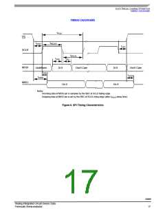
FUNCTIONAL DEVICE OPERATION
OPERATIONAL MODES
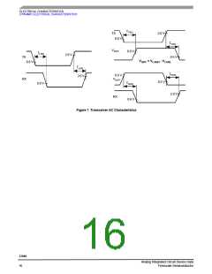
FUNCTIONAL DEVICE OPERATION
however, depending upon the PNP gain an external resistor-
DEVICE SUPPLY
capacitor network might be connected. The V2 is the supply
input for the CAN cell. The state of V2 is reported in the IOR
(bit V2LOW set to 1 if V2 is below 4.5 V typical).
The device is supplied from the battery line through the
VSUP pin. An external diode is required to protect against
negative transients and reverse battery. It can operate from
4.5 V and under the jump start condition at 27 Vdc. This pin
sustains standard automotive voltage conditions such as
load dump at 40 V. When VSUP falls below 3.0 V typical the
33989 detects it and stores the information into the SPI
register in a bit called BATFAIL. This detection is available in
all operation modes.
HS1 VBAT SWITCH OUTPUT
The HS1 output is a 2.0 Ω typical switch from the VSUP
pin. It allows the supply of external switches and their
associated pull-up or pull down circuitry, in conjunction with
the wake-up input pins, for example. Output current is limited
to 200 mA and HS1 is protected against short-circuit and has
an overtemperature shutdown (bit HS1OT in IOR and bit
HS1OT-V2LOW in INT register). The HS1 output is controlled
from the internal register and the SPI. Because of an internal
timer, it can be activated at regular intervals in Sleep and
Stop modes. It can also be permanently turned on in Normal
or Standby modes to drive loads or supply peripheral
components. No internal clamping protection circuit is
implemented, thus a dedicated external protection circuit is
required in case of inductive load drive.
The device incorporates a battery early warning function,
providing a maskable interrupt when the VSUP voltage is
below 6.0 V typical. A hysteresis is included. Operation is
only in Normal and Standby modes. VSUP low is reported in
the Input/Output Register (IOR).
VDD1 VOLTAGE REGULATOR
The VDD1 Regulator is a 5.0 V output voltage with output
current capability up to 200 mA. It includes a voltage
monitoring circuitry associated with a reset function. The
VDD1 regulator is fully protected against overcurrent and
short-circuit. It has over- temperature detection warning flags
(bit VDDTEMP in MCR and interrupt registers), and
overtemperature shutdown with hysteresis.
BATTERY FALL EARLY WARNING
Refer to the discussion under the heading: Device Supply.
INTERNAL CLOCK
V2 REGULATOR
The device has an internal clock used to generate all
timings (Reset, Watchdog, Cyclic Wake-up, Filtering Time,
etc.). Two oscillators are implemented. A high accuracy
(±12 percent) used in Normal Request, Normal and Standby
modes, and a low accuracy (±30 percent) used in Sleep and
Stop modes.
V2 Regulator circuitry is designed to drive an external path
transistor increasing output current flexibility. Two pins are
used to achieve the flexibility. Those pins are V2 and V2
control. The output voltage is 5.0 V and is realized by a
tracking function of the VDD1 regulator. The recommended
ballast transistor is MJD32C. Other transistors can be used;
OPERATIONAL MODES
wake-up input reading through SPI and HS1 activation. The
Watchdog is running.
FUNCTIONAL MODES
The device has four primary operation modes:
1. Standby mode
NORMAL MODE
2. Normal mode
In this mode both regulators are ON. This corresponds to
the normal application operation. All functions are available in
this mode (Watchdog, wake-up input reading through SPI,
HS1 activation, CAN communication). The software
Watchdog is running and must be periodically cleared
through SPI.
3. Stop mode
4. Sleep mode
All modes are controlled by the SPI. An additional
temporary mode called Normal Request mode is
automatically accessed by the device after reset or wake-up
from Stop mode. A Reset (RST) mode is also implemented.
Special modes and configuration are possible for debug and
program MCU flash memory.
STOP MODE
Regulator 2 is turned OFF by disabling the V2 control pin.
The regulator 1 is activated in a special low power mode,
allowing to deliver few mA. The objective is to maintain the
MCU of the application supplied while it is turned into power
saving condition (i.e Stop or Wait modes). In Stop mode the
device supply current from VBAT is very low.
STANDBY MODE
Only regulator 1 is ON. Regulator 2 is turned OFF by
disabling the V2 control pin. Only the wake-up capability of
the CAN interface is available. Other functions available are
33989
Analog Integrated Circuit Device Data
Freescale Semiconductor
20

 FREESCALE [ Freescale ]