FUNCTIONAL DEVICE OPERATION
OPERATIONAL MODES
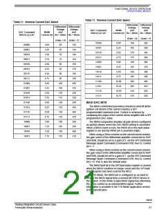
Table 11. Nominal Current DAC Select
Table 11. Nominal Current DAC Select
Differential Differential
Differential Differential
Voltage
(mV
Voltage
(mV
Voltage
(mV
Voltage
(mV
DAC Command
Bits<4,3,2,1,0>
NOMI
DAC Command
Bits<4,3,2,1,0>
NOMI
Current (A) Rs = 20mΩ Rs = 40mΩ
Current (A) Rs = 20mΩ Rs = 40mΩ
(Gain = 2)
160
(Gain = 1)
320
(Gain = 2)
60
(Gain = 1)
120
130
140
150
160
170
180
190
200
210
220
230
240
250
260
270
280
290
300
310
10100
10101
10110
10111
11000
11001
11010
11011
11100
11101
11110
11111
8.00
8.25
00000
00001
00010
00011
00100
00101
00110
00111
01000
01001
01010
01011
01100
01101
01110
01111
10000
10001
10010
10011
3.00
3.25
3.50
3.75
4.00
4.25
4.50
4.75
5.00
5.25
5.50
5.75
6.00
6.25
6.50
6.75
7.00
7.25
7.50
7.75
165
330
65
8.50
170
340
70
8.75
175
350
75
9.00
180
360
80
9.25
185
370
85
9.50
190
380
90
9.75
195
390
95
10.00
10.25
10.50
10.75
200
400
100
105
110
115
120
125
130
135
140
145
150
155
205
410
210
420
215
430
MAXI DAC BITS
The MAXI control block provides a means to shut off all the
ignition coil drivers if the current reaches a SPI
programmable maximum level. Control is achieved by
comparing the output of the current sense amplifier with a SPI
programmed DAC value.
The MAXI comparator disables all gate drivers configured
as ignition drivers when the DAC MAXI setting is exceeded.
When a MAXI event occurs, the MAXI bit in the fault status
register is set and the MAXI pin is asserted (High).
When using a 20mΩ resistor as the current sense resistor,
the gain select of the differential amplifier connected to RSP
and RSN, should be set to a gain of 2, via the SPI Command
Message Spark Command (Command 0100, hex 4), Control
bit 6 =1.
When using a 40mΩ resistor as the current sense resistor,
the gain select of the differential amplifier connected to RSP
and RSN, should be set to a gain of 1, via the SPI Command
Message Spark Command (Command 0100, hex 4), Control
bit 6 =0. This is also the default value.
The MAXI fault bit in the SPI fault status register is cleared
when the MAXI condition no longer exists and the SPI fault
status register has been read by the MCU.
In V10 Mode, the MAXI pin is configured as an input to
receive the MAXI signal from a second MC33810 device in
the system. In this mode a input MAXI signal has effectively
the same control as an internal MAXI signal. Further
information is provided in the V10 Mode application section
of this specification.
33810
Analog Integrated Circuit Device Data
Freescale Semiconductor
21

 FREESCALE [ Freescale ]