FUNCTIONAL DEVICE OPERATION
OPERATIONAL MODES
.
V10 MODE
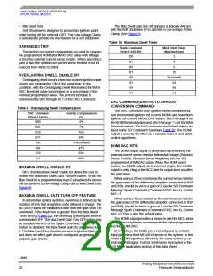
Table 16. Frequency Select
V10 Mode provides a method for monitoring 10 ignition
events while using only two current sense resistors. This is
achieved using three MC33810 devices. Two MC33810
devices are programmed as Normal Ignition mode outputs
and one is programmed as a V10 ignition mode output. The
ignition gate driver outputs are partitioned into two banks of
five outputs each (See Figure 10). Each bank contains one or
two driver(s) from the V10 device.
PWM Freq&DC
Command
Bit<b9,b8,b7>
Frequency Hz
000
001
010
011
100
101
110
111
10Hz (default)
20Hz
40Hz
Drivers in the V10 device are grouped in two’s (GD0&GD2,
GD1&GD3). Current from each V10 mode IGBT group is
monitored by the appropriate Normal Mode device (See
Figure 10). The MAXI signal from one Normal Mode device is
ported to the V10 Mode MAXI input pin. Likewise the MAXI
signal from the second Normal Mode device is ported to the
V10 Mode NOMI input pin. The V10 Mode NOMI/MAXI inputs
are used as MAXI shutdown signals for the appropriate
ignition gate drive group.
80Hz
160Hz
320Hz
640Hz
1.28kHz
V10 Mode contains the same features as Ignition Mode
gate drivers with the following exceptions:
Notes: Tolerance on selected frequency is ±10% after using the
Calibration Command. Shorts to battery and open load faults will not
be detected for frequency and duty cycle combinations inconsistent
with fault timers.
• NOMI/MAXI configured as input pins
• MAXI shutdown for GPGD disabled
• NOMI/MAXI comparators disabled
Table 17. Pre-driver GDx Output Control
In V10 Mode, Spark Command bits 7 and 8 (Gain Select,
Overlapping Dwell) are disabled. These two features are
achieved through the Normal Mode devices.
Mode
Driver
On/OFF
IGN/GP Bit GPGD Bit
PWMx
Enable Bit
GINx
terminal
GDx
Command
Output
RSN and RSP must be grounded in V10 Mode.
1
1
1
1
1
0
0
1
X
1
X
0
0
1
1
0
1
X
1
X
OFF
ON
ON
Freq/DC
Freq/DC
33810
Analog Integrated Circuit Device Data
Freescale Semiconductor
24

 FREESCALE [ Freescale ]