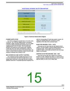
FUNCTIONAL DEVICE OPERATION
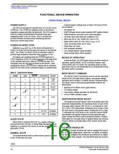
OPERATIONAL MODES
the MAXI shutdown signal for GD0 and GD2 and the new
NOMI input pin receives the MAXI shutdown signal for GD1
and GD3. Further information on V10 Mode is provided in the
V10 Application section.
IGNITION (IGBT) GATE DRIVER MODE
The MC33810 contains dedicated circuitry necessary for
automotive ignition control systems. Each gate driver may be
individually configured as an Ignition Gate Driver with the
following features:
Note: RSN and RSP must be grounded in V10 Mode.
OVER/UNDER-VOLTAGE SHUTDOWN/RETRY BIT
• Spark duration signal
The Over/Under-voltage Shutdown/Retry bit allows the
user to select the global over and under-voltage fault strategy
for all the outputs. In an over-voltage or under-voltage
condition on the VPWR pin, all outputs are commanded off.
The Over/Under-voltage control bit sets the operation of the
outputs when returning from over/under- voltage. Setting the
Over/Under-voltage bit to logic [1] will force all outputs to
remain OFF when VPWR returns to normal level. To turn the
output on again, the corresponding input pin or SPI bit must
be reactivated. Setting the Over/Under-voltage bit to logic [0]
will command all outputs to resume their previous state when
VPWR returns to normal level. Table 6 below provides the
output state when returning from over or under-voltage.
• Open secondary timer
• Soft shutdown control
• Low-voltage flyback clamp
• Ignition ignition coil current measurement
• MAXI output and control
• NOMI output
• Maximum dwell timer
In the Ignition Mode, several control strategies are in place
to control the IGBT for enhanced system performance.
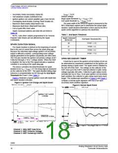
Information acquired from the FBx pin allows the device to
produce a spark duration signal output (SPKDUR) and detect
open secondary ignition coils. Based on the FBx signal and
Spark Command register settings, the device performs the
appropriate gate control (Low-voltage Flyback Clamp, Soft
Shutdown) and produces the SPKDUR output.
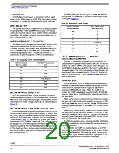
Table 6. Over-voltage/Under-voltage Truth Table
Over/
The FBx pin is connected to the collector of the IGBT
through an external 9:1 resistor divider network. The
recommended values for the resistor divider network is 36K
and 4.02K, with the 36K resistor connected from the IGBT
collector to the FBx pin and the 4.02K resistor connected
from the FBx pin to ground.
Under-
voltage
Control
Bit
State When
Returning From
Over/Under-voltage
GINx DINx
Input Pin
SPI
Bit
OUTEN
Input pin
OFF
OFF
OFF
ON
X
X
0
X
X
0
X
1
1
0
0
0
0
Additional controls to the gate driver are achieved by
sensing the current through the external IGBT. The Resistor
Sense Positive (RSP) and Resistor Sense Negative (RSN)
inputs are use to measure the voltage across an external
20mΩ or 40mΩ current sense resistor. A gain select bit in the
Spark Command SPI Command messages should be set to
1 (gain of 2) when using a 20mΩ current sense resistor.
When using a 40mΩ current sense resistor, the gain select bit
should be set to 0 (gain of 1 is the default value).
0*
0*
0*
X
1
1
ON
X
* Default Setting
Note: The SPI bit does not control the Gate Driver outputs in
the Ignition Mode, only in the GPGD Mode.
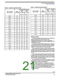
The ignition coil current is compared with the output of the
DACs which have been programmed via the SPI Commands.
The comparison generates the Nominal Current signal
(NOMI) and the Maximum Current signal (MAXI). Both
signals have a low output when the ignition coil current is
below the programmed DAC value and a high output when
the current is above the programmed DAC value.
An under-voltage condition on VDD results in the global
shutdown of all outputs and reset of all internal control
registers. The VDD under-voltage threshold is between 0.8V
and 2.8V
When the GDx output is shutdown because of the control
strategy, the output may be activated again by toggling the
input control.
PWM ENABLE BIT
X
Gate Driver outputs programmed as General Purpose
Gate Drivers may be used as low frequency PWM outputs.
The PWM generators are enabled via bits 0 through 3 in the
Mode Select Command. Bits 0 through 3 correspond to
outputs GD0 through GD3 respectively. Once the frequency
and duty cycle are programmed through the PWM Frequency
& DC command, the PWM output may be turned ON and
OFF through the PWM enable bit. Further information on
PWM control is provided in the General Purpose Gate Driver
Mode section of this data sheet.
SPARK COMMAND
The Spark Command is an ignition mode command used
to program the parameters for the ignition mode features
listed below:
• End spark threshold (EndSparkTh bits)
• Open secondary fault timer (OSFLT bits)
33810
Analog Integrated Circuit Device Data
Freescale Semiconductor
17

 FREESCALE [ Freescale ]