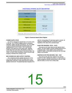
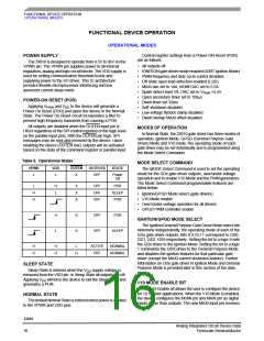
FUNCTIONAL DEVICE OPERATION
OPERATIONAL MODES
• Secondary clamp (secondary clamp bit)
• Soft shutdown enable (SoftShutDn bit)
VPWR = 16.0V
Default settings
Begin spark threshold VIH = VPWR + 21V
End spark threshold VIL = VPWR +5.5V
• Ignition ignition coil current amplifier gain (Gain Sel bit)
• Overlapping dwell disable (Overlap Dwell Disable bit)
• Maximum dwell enable (MaxDwellEn bit)
• Maximum dwell timer (MaxDwellTimer bits)
• End of spark filter timer value
The pulse width of the SPKDUR signal is measured by the
MCU timer/input capture port to determine the actual spark
duration. Spark duration information is then used by the MCU
spark control algorithm to optimize the dwell time.
Spark Command address and data bits are listed in
Table 20
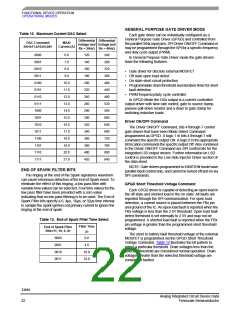
Table 7. End Spark Threshold
NOTE: Gate driver outputs programmed to be General
Purpose Gate Drivers are not affected by the Spark
Commands.
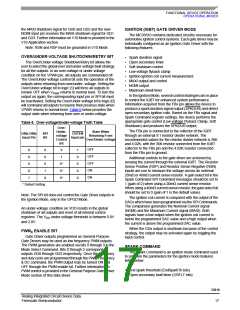
Spark Command
End Spark Threshold (VIL)
Bit<b1,b0>
00
01
10
11
VPWR + 2.75
VPWR + 5.5
VPWR + 8.2
VPWR + 11.0
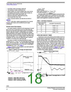
SPARK DURATION SIGNAL
The Spark Duration is defined as the beginning of current
flow to the end of current flow across the spark plug gap.
Because the extremely high-voltage ignition coil secondary
output is difficult to monitor, corresponding lower voltage
signals generated on the ignition coil primary are often used.
The FBx pins monitor the ignition coil primary voltage (IGBT
Collector) through a 10 to 1 voltage divider. When the IGBT
is disabled, the rise in the FBx signal indicates a sparkout
condition is occurring at the spark plug gap.
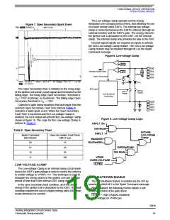
OPEN SECONDARY TIMER
A fault due to open in the ignition coil secondary circuit can
be determined by waveforms established on the ignition coil
primary during a spark event. The spark event is initiated by
the turn off of the IGBT. The voltage on the collector of the
IGBT rises up to the IGBT’s internal collector to gate clamp
voltage (typically 400 volts). Collector to gate clamp events
normally last 5µs to 50µs. In an open ignition coil secondary
fault condition, the collector to gate clamp event lasts much
longer. The oscilloscope waveform in Figure 6 and Figure 7
compare a normal spark signature with that of an open
secondary fault condition signature.
The device considers the initial thresholds for spark
duration to be VIH = VPWR + 21V for rising edge as measured
on the collector of the IGBT. The spark duration falling edge
reference is programmable via SPI through the End Spark
Threshold bits 0 and 1 (See Table 7).
Figure 5 illustrates a typical ignition event with dwell time
and spark duration indicated.
Figure 5. Ignition Coil Charge and Spark Event
Figure 6. Normal Spark Event
Ignition Coil Current,
5.0A/div
SPKDUR~3.0ms
DWELL Time
Channel 1: GINx IGBT Gate Drive
Channel 2: IGBT Collector Voltage
Channel 3: IGBT Current @ 5.0A/Div
33810
Analog Integrated Circuit Device Data
Freescale Semiconductor
18

 FREESCALE [ Freescale ]