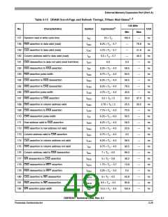
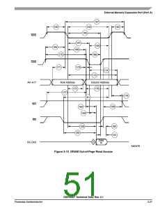
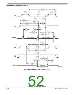
External Memory Expansion Port (Port A)
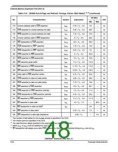
Table 3-13 DRAM Out-of-Page and Refresh Timings, Fifteen Wait States1, 2
100 MHz
No.
Characteristics
Symbol
Expression3
Unit
Min
Max
—
157 Random read or write cycle time
158 RAS assertion to data valid (read)
159 CAS assertion to data valid (read)
160 Column address valid to data valid (read)
161 CAS deassertion to data not valid (read hold time)
162 RAS deassertion to RAS assertion
163 RAS assertion pulse width
tRC
tRAC
tCAC
tAA
16 × TC
160.0
—
ns
ns
ns
ns
ns
ns
ns
ns
ns
ns
ns
ns
ns
ns
ns
ns
ns
ns
ns
ns
ns
ns
ns
ns
ns
ns
8.25 × TC − 5.7
4.75 × TC − 5.7
5.5 × TC − 5.7
0.0
76.8
41.8
49.3
—
—
—
tOFF
tRP
0.0
6.25 × TC − 4.0
9.75 × TC − 4.0
6.25 × TC − 4.0
8.25 × TC − 4.0
4.75 × TC − 4.0
58.5
93.5
58.5
78.5
43.5
33.0
25.5
73.5
56.5
58.5
23.5
3.5
—
tRAS
tRSH
tCSH
tCAS
tRCD
tRAD
tCRP
tCP
—
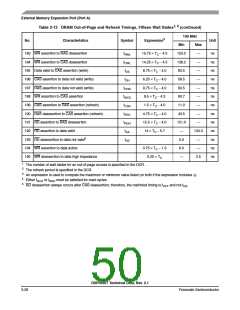
164 CAS assertion to RAS deassertion
165 RAS assertion to CAS deassertion
166 CAS assertion pulse width
—
—
—
167 RAS assertion to CAS assertion
168 RAS assertion to column address valid
169 CAS deassertion to RAS assertion
170 CAS deassertion pulse width
3.5 × TC
2
37.0
29.5
—
2.75 × TC
2
7.75 × TC − 4.0
6.25 × TC – 6.0
6.25 × TC − 4.0
2.75 × TC − 4.0
0.75 × TC − 4.0
6.25 × TC − 4.0
9.75 × TC − 4.0
7 × TC − 4.0
—
171 Row address valid to RAS assertion
172 RAS assertion to row address not valid
173 Column address valid to CAS assertion
174 CAS assertion to column address not valid
175 RAS assertion to column address not valid
176 Column address valid to RAS deassertion
177 WR deassertion to CAS assertion
178 CAS deassertion to WR4 assertion
179 RAS deassertion to WR4 assertion
180 CAS assertion to WR deassertion
181 RAS assertion to WR deassertion
182 WR assertion pulse width
tASR
tRAH
tASC
tCAH
tAR
—
—
—
58.5
93.5
66.0
46.2
13.8
0.5
—
—
tRAL
tRCS
tRCH
tRRH
tWCH
tWCR
tWP
—
5 × TC − 3.8
—
1.75 × TC – 3.7
0.25 × TC − 2.0
6 × TC − 4.2
—
—
55.8
90.8
150.5
—
9.5 × TC − 4.2
15.5 × TC − 4.5
—
—
DSP56367 Technical Data, Rev. 2.1
Freescale Semiconductor
3-25

 FREESCALE [ Freescale ]