External Memory Expansion Port (Port A)
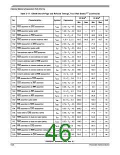
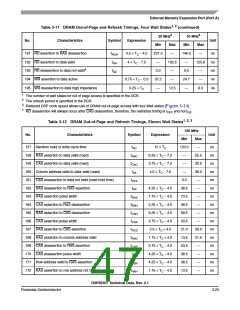
Table 3-11 DRAM Out-of-Page and Refresh Timings, Four Wait States1, 2 (continued)
20 MHz3 30 MHz3
No.
Characteristics
Symbol
Expression
Unit
Min
Max
—
Min
Max
—
191 RD assertion to RAS deassertion
192 RD assertion to data valid
tROH
tGA
4.5 × TC − 4.0
4 × TC − 7.5
221.0
—
146.0
—
ns
ns
ns
ns
ns
192.5
—
125.8
—
193 RD deassertion to data not valid4
194 WR assertion to data active
tGZ
0.0
0.0
0.75 × TC − 0.3
0.25 × TC
37.2
—
—
24.7
—
—
195 WR deassertion to data high impedance
12.5
8.3
1
2
3
4
The number of wait states for out of page access is specified in the DCR.
The refresh period is specified in the DCR.
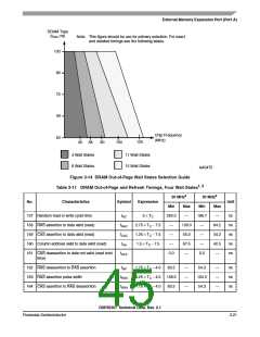
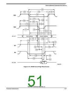
Reduced DSP clock speed allows use of DRAM out-of-page access with four Wait states (Figure 3-14).
RD deassertion will always occur after CAS deassertion; therefore, the restricted timing is tOFF and not tGZ
.
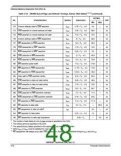
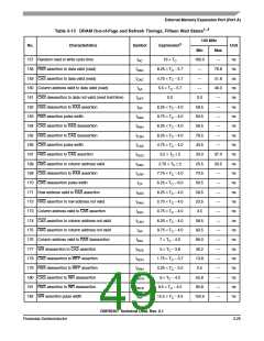
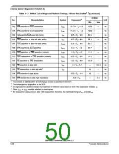
Table 3-12 DRAM Out-of-Page and Refresh Timings, Eleven Wait States1, 2, 3
100 MHz
No.
Characteristics
Symbol
Expression
Unit
Min
120.0
—
Max
—
157 Random read or write cycle time
158 RAS assertion to data valid (read)
159 CAS assertion to data valid (read)
160 Column address valid to data valid (read)
161 CAS deassertion to data not valid (read hold time)
162 RAS deassertion to RAS assertion
163 RAS assertion pulse width
tRC
tRAC
tCAC
tAA
12 × TC
ns
ns
ns
ns
ns
ns
ns
ns
ns
ns
ns
ns
ns
ns
ns
ns
6.25 × TC − 7.0
3.75 × TC − 7.0
4.5 × TC − 7.0
55.5
30.5
38.0
—
—
—
tOFF
tRP
0.0
4.25 × TC − 4.0
7.75 × TC − 4.0
5.25 × TC − 4.0
6.25 × TC − 4.0
3.75 × TC − 4.0
2.5 × TC 4.0
1.75 × TC 4.0
5.75 × TC − 4.0
4.25 × TC − 4.0
4.25 × TC − 4.0
1.75 × TC − 4.0
38.5
73.5
48.5
58.5
33.5
21.0
13.5
53.5
38.5
38.5
13.5
—
tRAS
tRSH
tCSH
tCAS
tRCD
tRAD
tCRP
tCP
—
164 CAS assertion to RAS deassertion
165 RAS assertion to CAS deassertion
166 CAS assertion pulse width
—
—
—
167 RAS assertion to CAS assertion
168 RAS assertion to column address valid
169 CAS deassertion to RAS assertion
170 CAS deassertion pulse width
29.0
21.5
—
—
171 Row address valid to RAS assertion
172 RAS assertion to row address not valid
tASR
tRAH
—
—
DSP56367 Technical Data, Rev. 2.1
Freescale Semiconductor
3-23

 FREESCALE [ Freescale ]