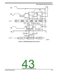
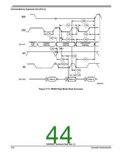
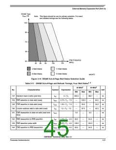
External Memory Expansion Port (Port A)
DRAM Type
(tRAC ns)
Note: This figure should be use for primary selection. For exact
and detailed timings see the following tables.
100
80
70
60
50
Chip Frequency
(MHz)
120
40
66
80
100
4 Wait States
8 Wait States
11 Wait States
15 Wait States
AA0475
Figure 3-14 DRAM Out-of-Page Wait States Selection Guide
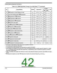
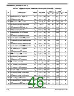
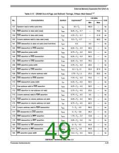
Table 3-11 DRAM Out-of-Page and Refresh Timings, Four Wait States1, 2
20 MHz3 30 MHz3
No.
Characteristics
Symbol
Expression
Unit
Min
Max
—
Min
166.7
—
Max
—
157 Random read or write cycle time
158 RAS assertion to data valid (read)
159 CAS assertion to data valid (read)
160 Column address valid to data valid (read)
tRC
tRAC
tCAC
tAA
5 × TC
250.0
—
ns
ns
ns
ns
ns
2.75 × TC − 7.5
1.25 × TC − 7.5
1.5 × TC − 7.5
130.0
55.0
67.5
—
84.2
34.2
42.5
—
—
—
—
—
161 CAS deassertion to data not valid (read hold
time)
tOFF
0.0
0.0
162 RAS deassertion to RAS assertion
163 RAS assertion pulse width
tRP
1.75 × TC − 4.0
3.25 × TC − 4.0
1.75 × TC − 4.0
83.5
158.5
83.5
—
—
—
54.3
104.3
54.3
—
—
—
ns
ns
ns
tRAS
tRSH
164 CAS assertion to RAS deassertion
DSP56367 Technical Data, Rev. 2.1
Freescale Semiconductor
3-21

 FREESCALE [ Freescale ]