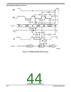
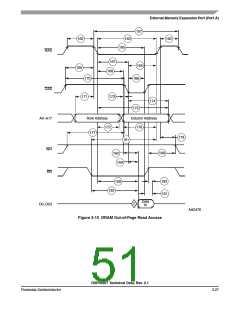
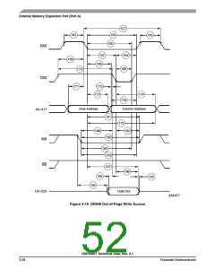
External Memory Expansion Port (Port A)
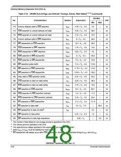
Table 3-12 DRAM Out-of-Page and Refresh Timings, Eleven Wait States1, 2, 3 (continued)
100 MHz
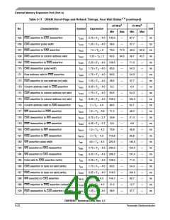
No.
Characteristics
Symbol
Expression
Unit
Min
3.5
Max
—
—
—
—
—
—
—
—
—
—
—
—
—
—
—
—
—
—
—
93.0
—
—
2.5
173 Column address valid to CAS assertion
174 CAS assertion to column address not valid
175 RAS assertion to column address not valid
176 Column address valid to RAS deassertion
177 WR deassertion to CAS assertion
178 CAS deassertion to WR4 assertion
179 RAS deassertion to WR4 assertion
180 CAS assertion to WR deassertion
181 RAS assertion to WR deassertion
182 WR assertion pulse width
tASC
tCAH
tAR
0.75 × TC − 4.0
5.25 × TC − 4.0
7.75 × TC − 4.0
6 × TC − 4.0
ns
ns
ns
ns
ns
ns
ns
ns
ns
ns
ns
ns
ns
ns
ns
ns
ns
ns
ns
ns
ns
ns
ns
48.5
73.5
56.0
26.0
13.5
0.5
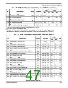
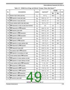
tRAL
tRCS
tRCH
tRRH
tWCH
tWCR
tWP
3.0 × TC − 4.0
1.75 × TC − 4.0
0.25 × TC − 2.0
5 × TC − 4.2
45.8
70.8
110.5
113.2
103.2
53.5
48.5
73.5
60.7
11.0
23.5
111.0
—
7.5 × TC − 4.2
11.5 × TC − 4.5
11.75 × TC − 4.3
10.25 × TC − 4.3
5.75 × TC − 4.0
5.25 × TC − 4.0
7.75 × TC − 4.0
6.5 × TC − 4.3
1.5 × TC − 4.0
2.75 × TC − 4.0
11.5 × TC − 4.0
10 × TC − 7.0
183 WR assertion to RAS deassertion
184 WR assertion to CAS deassertion
185 Data valid to CAS assertion (write)
186 CAS assertion to data not valid (write)
187 RAS assertion to data not valid (write)
188 WR assertion to CAS assertion
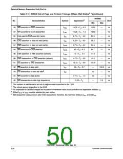
tRWL
tCWL
tDS
tDH
tDHR
tWCS
tCSR
tRPC
tROH
tGA
189 CAS assertion to RAS assertion (refresh)
190 RAS deassertion to CAS assertion (refresh)
191 RD assertion to RAS deassertion
192 RD assertion to data valid
193 RD deassertion to data not valid5
194 WR assertion to data active
tGZ
0.0
0.75 × TC − 0.3
0.25 × TC
7.2
195 WR deassertion to data high impedance
—
1
2
3
4
5
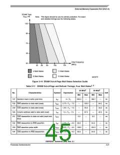
The number of wait states for out-of-page access is specified in the DCR.
The refresh period is specified in the DCR.
The asynchronous delays specified in the expressions are valid for DSP56367.
Either tRCH or tRRH must be satisfied for read cycles.
RD deassertion will always occur after CAS deassertion; therefore, the restricted timing is tOFF and not tGZ
.
DSP56367 Technical Data, Rev. 2.1
3-24
Freescale Semiconductor

 FREESCALE [ Freescale ]