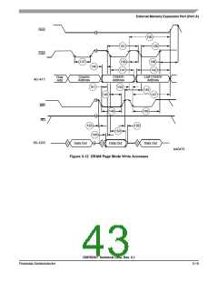
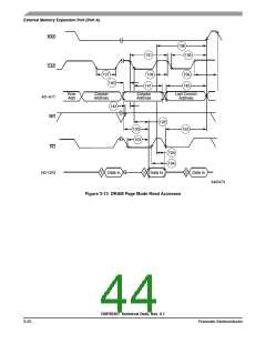
External Memory Expansion Port (Port A)
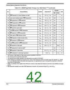
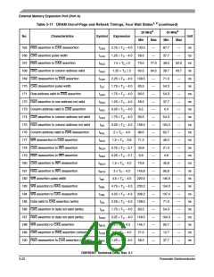
Table 3-10 DRAM Page Mode Timings, Four Wait States1, 2, 3 (continued)
100 MHz
Min Max
No.
Characteristics
Symbol
Expression4
Unit
141 CAS assertion to column address not valid
142 Last column address valid to RAS deassertion
143 WR deassertion to CAS assertion
144 CAS deassertion to WR assertion
145 CAS assertion to WR deassertion
146 WR assertion pulse width
tCAH
tRAL
tRCS
tRCH
tWCH
tWP
3.5 × TC − 4.0
5 × TC − 4.0
31.0
46.0
8.5
—
—
ns
ns
ns
ns
ns
ns
ns
ns
ns
ns
ns
ns
ns
ns
ns
ns
1.25 × TC − 4.0
1.25 × TC – 3.7
3.25 × TC − 4.2
4.5 × TC − 4.5
4.75 × TC − 4.3
3.75 × TC − 4.3
0.5 × TC – 4.5
3.5 × TC − 4.0
1.25 × TC − 4.3
4.5 × TC − 4.0
3.25 × TC − 5.7
—
8.8
—
28.3
40.5
43.2
33.2
0.5
—
—
147 Last WR assertion to RAS deassertion
148 WR assertion to CAS deassertion
149 Data valid to CAS assertion (write)
150 CAS assertion to data not valid (write)
151 WR assertion to CAS assertion
152 Last RD assertion to RAS deassertion
153 RD assertion to data valid
tRWL
tCWL
tDS
—
—
—
tDH
31.0
8.2
—
tWCS
tROH
tGA
—
41.0
—
—
26.8
—
154 RD deassertion to data not valid6
155 WR assertion to data active
tGZ
0.0
0.75 × TC – 1.5
0.25 × TC
6.0
—
156 WR deassertion to data high impedance
—
2.5
1
2
3
4
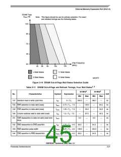
The number of wait states for Page mode access is specified in the DCR.
The refresh period is specified in the DCR.
The asynchronous delays specified in the expressions are valid for DSP56367.
All the timings are calculated for the worst case. Some of the timings are better for specific cases (for example, tPC equals
3 × TC for read-after-read or write-after-write sequences). An expressions is used to calculate the maximum or minimum
value listed, as appropriate.
5
6
BRW[1–0] (DRAM control register bits) defines the number of wait states that should be inserted in each DRAM out-of-page
access.
RD deassertion always occurs after CAS deassertion; therefore, the restricted timing is tOFF and not tGZ
.
DSP56367 Technical Data, Rev. 2.1
3-18
Freescale Semiconductor

 FREESCALE [ Freescale ]