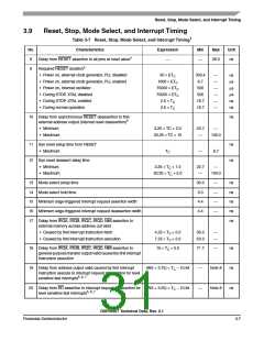
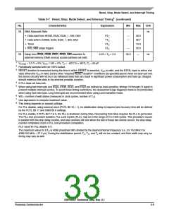
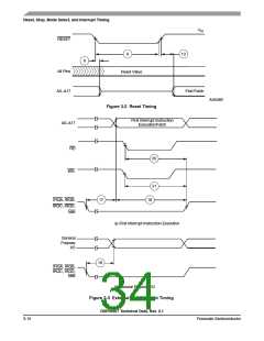
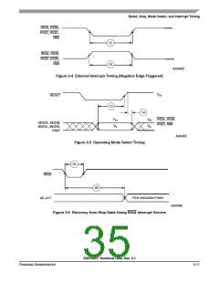
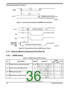
Reset, Stop, Mode Select, and Interrupt Timing
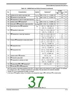
Table 3-7 Reset, Stop, Mode Select, and Interrupt Timing1 (continued)
No.
Characteristics
Expression
Min
Max
Unit
28 DMA Requests Rate
ns
• Data read from HDI08, ESAI, ESAI_1, SHI, DAX
• Data write to HDI08, ESAI, ESAI_1, SHI, DAX
• Timer
6TC
7TC
2TC
3TC
—
—
40.0
46.7
13.3
20.0
• IRQ, NMI (edge trigger)
—
29 Delay from IRQA, IRQB, IRQC, IRQD, NMI assertion to
external memory (DMA source) access address out valid
4.25 × TC + 2.0
30.3
—
ns
1
2
3
VCCQH = 3.3 V 5%; VCC= 1.8V 5%; TJ = –40°C to + 95°C, CL = 50 pF
Periodically sampled and not 100% tested.
RESET duration is measured during the time in which RESET is asserted, VCC is valid, and the EXTAL input is active and
valid. When the VCC is valid, but the other “required RESET duration” conditions (as specified above) have not been yet met,
the device circuitry will not be in an initialized state that can result in significant power consumption and heat-up. Designs
should minimize this state to the shortest possible duration.
4
5
If PLL does not lose lock.
When using fast interrupts and IRQA, IRQB, IRQC, and IRQD are defined as level-sensitive, timings 19 through 21 apply to
prevent multiple interrupt service. To avoid these timing restrictions, the deasserted Edge-triggered mode is recommended
when using fast interrupts. Long interrupts are recommended when using Level-sensitive mode.
6
7
8
WS = number of wait states (measured in clock cycles, number of TC).
Use expression to compute maximum value.
This timing depends on several settings:
For PLL disable, using external clock (PCTL Bit 16 = 1), no stabilization delay is required and recovery time will be defined
by the PCTL Bit 17 and OMR Bit 6 settings.
For PLL enable, if PCTL Bit 17 is 0, the PLL is shutdown during Stop. Recovering from Stop requires the PLL to get locked.
The PLL lock procedure duration, PLL Lock Cycles (PLC), may be in the range of 0 to 1000 cycles. This procedure occurs
in parallel with the stop delay counter, and stop recovery will end when the last of these two events occurs: the stop delay
counter completes count or PLL lock procedure completion.
PLC value for PLL disable is 0.
The maximum value for ETC is 4096 (maximum MF) divided by the desired internal frequency (i.e., for 150 MHz it is
4096/150 MHz = 27.3 µs). During the stabilization period, TC, TH, and TL will not be constant, and their width may vary, so
timing may vary as well.
DSP56367 Technical Data, Rev. 2.1
Freescale Semiconductor
3-9

 FREESCALE [ Freescale ]