External Memory Expansion Port (Port A)
26
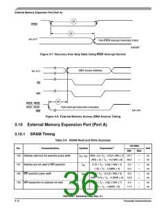
IRQA
25
A0–A17
First IRQA Interrupt Instruction Fetch
AA0467
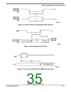
Figure 3-7 Recovery from Stop State Using IRQA Interrupt Service
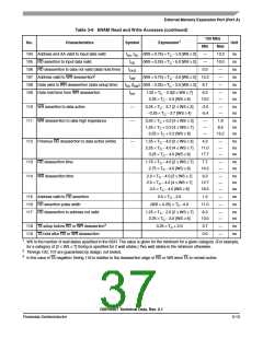
DMA Source Address
A0–A17
RD
WR
29
IRQA, IRQB,
IRQC, IRQD,
NMI
First Interrupt Instruction Execution
AA1104
Figure 3-8 External Memory Access (DMA Source) Timing
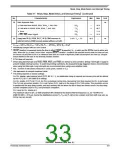
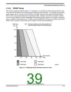
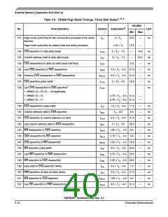
3.10 External Memory Expansion Port (Port A)
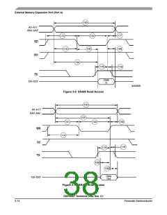
3.10.1 SRAM Timing
Table 3-8 SRAM Read and Write Accesses
150 MHz
No.
Characteristics
Symbol
Expression1
Unit
Min
Max
100 Address valid and AA assertion pulse width
101 Address and AA valid to WR assertion
102 WR assertion pulse width
tRC, tWC (WS + 2) × TC − 4.0 [2 ≤ WS ≤ 7] 22.7
—
—
ns
ns
(WS + 3) × TC − 4.0 [WS ≥ 8]
69.3
tAS
tWP
tWR
0.75 × TC − 2.0[2 ≤ WS ≤ 3]
1.25 × TC − 2.0[WS ≥ 4]
3.0
6.3
—
—
ns
ns
WS × TC − 4.0 [2 ≤ WS ≤ 3]
9.3
—
—
ns
ns
(WS − 0.5) × TC − 4.0[WS ≥ 4]
19.3
103 WR deassertion to address not valid
1.25 × TC − 4.0[2 ≤ WS ≤ 7]
2.25 × TC − 4.0[WS ≥ 8]
4.3
—
—
ns
ns
11.0
DSP56367 Technical Data, Rev. 2.1
3-12
Freescale Semiconductor

 FREESCALE [ Freescale ]