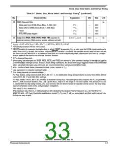
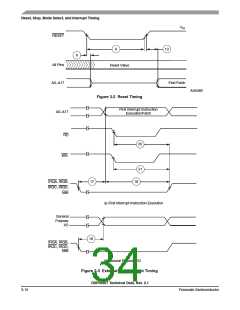
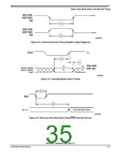
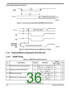
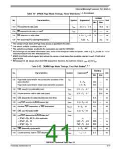
External Memory Expansion Port (Port A)
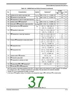
Table 3-8 SRAM Read and Write Accesses (continued)
Characteristics Symbol
Expression1
tAA, tAC (WS + 0.75) × TC − 5.0 [WS ≥ 2]
150 MHz
No.
Unit
Min
Max
13.3
10.0
—
104 Address and AA valid to input data valid
105 RD assertion to input data valid
—
—
ns
ns
ns
ns
ns
tOE
tOHZ
tAW
(WS + 0.25) × TC − 5.0 [WS ≥ 2]
106 RD deassertion to data not valid (data hold time)
107 Address valid to WR deassertion2
0.0
(WS + 0.75) × TC − 4.0 [WS ≥ 2] 14.3
—
108 Data valid to WR deassertion (data setup time)
109 Data hold time from WR deassertion
tDS (tDW) (WS − 0.25) × TC − 3.0 [WS ≥ 2]
8.7
—
tDH
1.25 × TC − 2.0[2 ≤ WS ≤ 7]
2.25 × TC − 2.0 [WS ≥ 8]
6.3
—
—
ns
ns
13.0
110 WR assertion to data active
—
0.25 × TC − 3.7 [2 ≤ WS ≤ 3]
−0.25 × TC − 3.7 [WS ≥ 4]
-2.0
-5.4
—
—
ns
ns
111 WR deassertion to data high impedance
—
0.25 × TC + 0.2 [2 ≤ WS ≤ 3]
1.25 × TC + 0.2 [4 ≤ WS ≤ 7]
2.25 × TC + 0.2 [WS ≥ 8]
—
—
—
1.9
8.5
ns
ns
ns
15.2
112 Previous RD deassertion to data active (write)
—
1.25 × TC − 4.0 [2 ≤ WS ≤ 3]
2.25 × TC − 4.0 [4 ≤ WS ≤ 7]
3.25 × TC − 4.0 [WS ≥ 8]
4.3
—
—
—
ns
ns
ns
11.0
17.7
113 RD deassertion time
114 WR deassertion time
1.75 × TC − 4.0 [2 ≤ WS ≤ 7]
2.75 × TC − 4.0 [WS ≥ 8]
7.7
—
—
ns
ns
14.3
2.0 × TC − 4.0 [2 ≤ WS ≤ 3]
2.5 × TC − 4.0 [4 ≤ WS ≤ 7]
3.5 × TC − 4.0 [WS ≥ 8]
9.3
—
—
—
ns
ns
ns
12.7
19.3
115 Address valid to RD assertion
116 RD assertion pulse width
0.5 × TC − 2.0
1.3
—
—
ns
ns
(WS + 0.25) × TC −4.0
11.0
117 RD deassertion to address not valid
1.25 × TC − 2.0 [2 ≤ WS ≤ 7]
2.25 × TC − 2.0 [WS ≥ 8]
6.3
—
—
ns
ns
13.0
118 TA setup before RD or WR deassertion3
119 TA hold after RD or WR deassertion
0.25 × TC + 2.0
3.7
0.0
—
—
ns
ns
1
WS is the number of wait states specified in the BCR. The value is given for the minimum for a given category. (For example,
for a category of [2 ≤ WS ≤ 7] timing is specified for 2 wait states.) Two wait states is the minimum otherwise.
Timings 100, 107 are guaranteed by design, not tested.
2
3
In the case of TA negation: timing 118 is relative to the deassertion edge of RD or WR were TA to remain active.
DSP56367 Technical Data, Rev. 2.1
Freescale Semiconductor
3-13

 FREESCALE [ Freescale ]