Freescale Semiconductor, Inc.
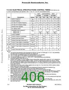
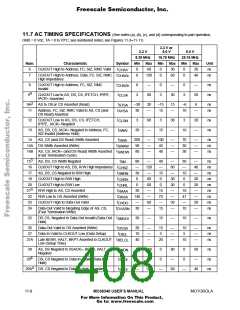
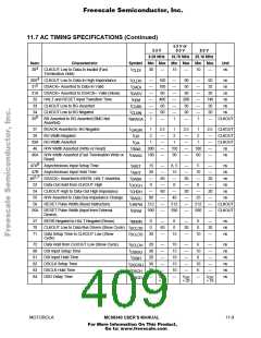
11.6 AC ELECTRICAL SPECIFICATIONS CONTROL TIMING (See notes (a), (b),
(c), and (d) corresponding to part operation, GND = 0 Vdc, TA = 0 to 70°C; see numbered notes)
3.3 V
3.3 V or 5.0 V
16.78 MHz
5.0 V
8.39 MHz
25.16 MHz
Num.
Characteristic
Symbol
Min
Max
Min
Max
Min
Max
25.16 MHz
50 kHz
Unit
1
System Frequency
f
dc
25
0.13
0.1
0
8.39
dc
16.78
dc
sys
Crystal Frequency
f
50
8.39
16.78
8
25
50
25
XTAL
On-Chip VCO System Frequency
On-Chip VCO Frequency Range
External Clock Operation
f
0.13 16.78 0.13 25.16 MHz
sys
f
0.1
0
33.5
16
0.1
0
50.3
25
MHz
MHz
ms
VCO
f
sys
2
PLL Start-up Time
t
—
20
—
20
—
20
rc
3
Limp Mode Clock Frequency
f
kHz
limp
SYNCR X-bit = 0
SYNCR X-bit = 1
—
—
f
/2
sys
—
—
f
/2
sys
—
—
f
/2
sys
sys
sys
sys
f
f
f
4
CLKOUT stability
∆
–1
119.2
125
125
56
+1
—
—
—
—
—
—
–1
59.6
62.5
62.5
28
+1
–1
40
40
40
19
18
20
+1
%
ns
ns
ns
ns
ns
ns
CLK
5
1
CLKOUT Period in Crystal Mode
External Clock Input Period
t
—
—
—
—
—
—
—
—
—
—
—
—
cyc
6
t
t
1B
EXTcyc
EXTcyc
7
External Clock Input Period with PLL
CLKOUT Pulse Width in Crystal Mode
CLKOUT Pulse Width in External Mode
1C
8
t
2,3
CW
9
t
t
56
28
2B, 3B
EXTCW
EXTCW
CLKOUT Pulse Width in External w/PLL
Mode
62.5
31
2C,
10
3C
CLKOUT Rise and Fall Times
t
—
10
—
5
—
4
ns
4,5
Crf
NOTES:
(a) The electrical specifications in this document for both the 8.39 and 16.78 MHz @ 3.3 V ±0.3 V are preliminary
and apply only to the appropriate MC68340V low voltage part.
(b) The 16.78-MHz specifications apply to the MC68340 @ 5.0 V ±5% operation.
(c) The 25.16 MHz @ 5.0 V ±5% electrical specifications are preliminary.
(d) For extended temperature parts T = –40 to +85°C. These specifications are preliminary.
A
1. All internal registers retain data at 0 Hz.
2. Assumes that a stable V
is applied, that an external filter capacitor with a value of 0.1 µF is attached to
CCSYN
the XFC pin, and that the crystal oscillator is stable. Lock time is measured from power-up to RESET release.
This specification also applies to the period required for PLL lock after changing the W and Y frequency control
bits in the synthesizer control register (SYNCR) while the PLL is running, and to the period required for the clock
to lock after LPSTOP.
3. Determined by the initial control voltage applied to the on-chip VCO. The X-bit in the SYNCR controls a divide-
by-two scaler on the system clock output.
4. CLKOUT stability is the average deviation from programmed frequency measured at maximum f
Measurement is made with a stable external clock input applied using the PLL.
.
sys
5. All crystal mode clock specifications are based on using a 32.768-kHz crystal for the input.
6. When using the external clock input mode (MODCK reset value = 0 V), the minimum allowable t
period
EXTcyc
will be reduced when the duty cycle of the signal applied to EXTAL exceeds 5% tolerance. The relationship
between external clock input duty cycle and minimum t is expressed:
EXTcyc
/ (50% – external clock input duty cycle tolerance).
Minimum external clock low and high times are based on a 45% duty cycle.
7. When using the external clock input mode with the PLL (MODCK reset value = 0 V), the external clock input duty
cycle can be at minimum 20% to produce a CLKOUT with a 50% duty cycle.
Minimum t
period = minimum t
EXTcyc
EXTCW
8. For crystal mode operation, the minimum CLKOUT pulse width is based on a 47% duty cycle.
9. For external clock mode operation, the minimum CLKOUT pulse width is based on a 45% duty cycle, with a 50%
duty cycle input clock.
11-6
MC68340 USER’S MANUAL
MOTOROLA
For More Information On This Product,
Go to: www.freescale.com

 FREESCALE [ Freescale ]