Freescale Semiconductor, Inc.
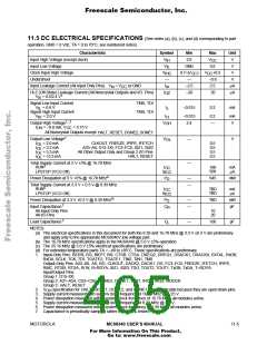
11.5 DC ELECTRICAL SPECIFICATIONS (See notes (a), (b), (c), and (d) corresponding to part
operation, GND = 0 Vdc, TA = 0 to 70°C; see numbered notes)
Characteristic
Input High Voltage (except clock)
Symbol
Min
2.0
Max
Unit
V
V
IH
V
CC
0.8
+0.3
Input Low Voltage
V
IL
GND
V
Clock Input High Voltage
Undershoot
V
IHC
—
0.7 (V
)
V
V
*
CC
CC
—
–0.8
2.5
20
V
Input Leakage Current (All Input Only Pins)
V
in
= V
CC
or GND
I
–2.5
–20
µA
µA
in
Hi-Z (Off-State) Leakage Current (All Noncrystal Outputs and I/O Pins)
I
OZ
1
V
= 0.5/2.4 V
in
Signal Low Input Current
= 0.8 V
TMS, TDI
TMS, TDI
V
I
–0.015
0.2
mA
IL
Signal High Input Current
= 2.0 V
L
V
I
–0.015
2.4
0.2
—
mA
V
IH
Output High Voltage
= –0.8 mA, V
H
1, 2
V
OH
I
= 4.75 V
CC
OH
All Noncrystal Outputs except HALT, RESET, DONE2, DONE1
1
Output Low Voltage
V
—
—
V
OL
I
I
I
I
= 2.0 mA
= 3.2 mA
= 5.3 mA
= 15.3 mA
CLKOUT, FREEZE, IPIPE, IFETCH
A23–A0, D15–D0, FC3–FC0, SIZ1, SIZ0
All Other Output Only and Group 2 I/O Pins
HALT, RESET
0.5
0.5
0.5
0.5
OL
OL
OL
OL
Total Supply Current at 5 V +5% @ 16.78 MHz
3
RUN
I
S
180
500
mA
µA
CC
LPSTOP (VCO Off)
ICC
4
Power Dissipation at 5 V +5% @ 16.78 MHz
P
—
—
945
mW
D
Total Supply Current at 3.3 V + 0.3 V @ 8.39 MHz
5
RUN
I
S
TBD
TBD
mA
µA
CC
LPSTOP (VCO Off)
ICC
6
Power Dissipation at 3.3 V +0.3 V @ 8.39 MHz
P
—
—
TBD
mW
pF
D
7
Input Capacitance
C
in
All Input-Only Pins
All I/O Pins
10
20
7
Load Capacitance
C
L
—
100
pF
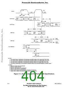
NOTES:
(a) The electrical specifications in this document for both the 8.39 and 16.78 MHz @ 3.3 V ±0.3 V are preliminary
and apply only to the appropriate MC68340V low voltage part.
(b) The 16.78-MHz specifications apply to the MC68340 @ 5.0 V ±5% operation.
(c) The 25.16 MHz @ 5.0 V ±5% electrical specifications are preliminary.
(d) For extended temperature parts TA = –40 to +85°C. These specifications are preliminary.
1. Input-Only Pins: BERR, BG, BKPT, BR, CTSB, CTSA, DREQ2, DREQ1, DSACK1, DSACK0, EXTAL, RxDB,
RxDA, SCLK, TCK, TDI, TGATE2, TGATE1, TIN2, TIN1, TMS
Output-Only Pins: A23–A0, AS, BG, CLKOUT, DACK2, DACK1, DS, FC3–FC0, FREEZE, IFETCH, IPIPE,
RMC, RTSB, RTSA, R/W, R≈RDYA, SIZ1, SIZ0, TDO, TOUT2, TOUT1, TxDB, TxDA, T≈RDYA
Input/Output Pins:
Group 1: D15–D0
Group 2: A31–A24, CS3–CS0, DONE2, DONE1, IRQ7, IRQ5, IRQ3, MODCK
Group 3: HALT, RESET
2.
V
OH
specification for HALT, RESET, DONE2, and DONE1 is not applicable because they are open-drain pins.
3. Supply current measured with system clock frequency of 16.78 MHz @ 5.25 V.
4. Power dissipation measured with a system clock frequency of 16.78 MHz, all modules active.
5. Supply current measured with system clock frequency of 8.39 MHz @ 3.6 V.
6. Power dissipation measured with a system clock frequency of 8.39 MHz, all modules active.
7. Capacitance is periodically sampled rather than 100% tested.
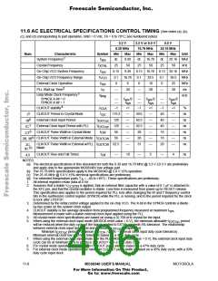
MOTOROLA
MC68340 USER’S MANUAL
11-5
For More Information On This Product,
Go to: www.freescale.com

 FREESCALE [ Freescale ]