Freescale Semiconductor, Inc.
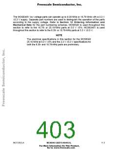
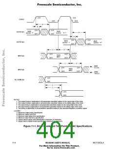
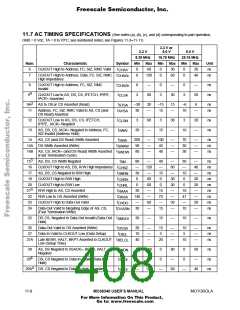
2.0 V
2.0 V
0.8 V
CLKOUT
0.8 V
A
B
2.0 V
0.8 V
2.0 V
0.8 V
VALID
OUTPUT
VALID
OUTPUT
OUTPUTS(1)
OUTPUTS(2)
A
n
n + 1
B
2.0 V
0.8 V
2.0 V
0.8 V
VALID
OUTPUT
VALID
OUTPUT
n
n+1
C
2.0 V
0.8 V
D
2.0 V
0.8 V
VALID
INPUT
INPUTS(3)
C
D
DRIVE
2.0 V
0.8 V
2.0 V
0.8 V
TO 2.4 V
VALID
INPUT
INPUTS(4)
DRIVE
TO 0.5 V
2.0 V
0.8 V
ALL SIGNALS(5)
E
F
2.0 V
0.8 V
NOTES:
1. This output timing is applicable to all parameters specified relative to the rising edge of the clock.
2. This output timing is applicable to all parameters specified relative to the falling edge of the clock.
3. This input timing is applicable to all parameters specified relative to the rising edge of the clock.
4. This input timing is applicable to all parameters specified relative to the falling edge of the clock.
5. This timing is applicable to all parameters specified relative to the assertion/negation of another signal.
LEGEND:
A. Maximum output delay specification.
B. Minimum output hold time.
C. Minimum input setup time specification.
D. Minimum input hold time specification.
E. Signal valid to signal valid specification (maximum or minimum).
F. Signal valid to signal invalid specification (maximum or minimum).
Figure 11-1. Drive Levels and Test Points for AC Specifications
11-4
MC68340 USER’S MANUAL
MOTOROLA
For More Information On This Product,
Go to: www.freescale.com

 FREESCALE [ Freescale ]