Freescale Semiconductor, Inc.
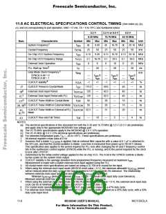
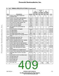
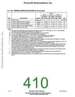
11.7 AC TIMING SPECIFICATIONS (Continued)
3.3 V or
5.0 V
3.3 V
5.0 V
8.39 MHz
16.78 MHz 25.16 MHz
Num.
85
Characteristic
Symbol Min Max Min Max Min Max
Unit
DSCLK Cycle
t
2
0
0
0
0
—
2
0
0
0
0
—
50
50
50
50
2
0
0
0
0
—
35
35
35
35
CLKOUT
DSCCYC
86
CLKOUT High to FREEZE Asserted
CLKOUT High to FREEZE Negated
CLKOUT High to IFETCH High Impedance
CLKOUT High to IFETCH Valid
t
100
100
100
100
ns
ns
ns
ns
FRZA
87
t
FRZN
88
t
IFZ
89
t
IF
NOTES:
(a) The electrical specifications in this document for both the 8.39 and 16.78 MHz @ 3.3 V ±0.3 V are preliminary
and apply only to the appropriate MC68340V low voltage part.
(b) The 16.78-MHz specifications apply to the MC68340 @ 5.0 V ±5% operation.
(c) The 25.16 MHz @ 5.0 V ±5% electrical specifications are preliminary.
(d) For extended temperature parts T = –40 to +85°C. These specifications are preliminary.
A
1. All AC timing is shown with respect to 0.8 V and 2.0 V levels unless otherwise noted.
2. This number can be reduced to 5 ns if strobes have equal loads.
3. If multiple chip selects are used, the CS width negated (#15) applies to the time from the negation of a heavily
loaded chip select to the assertion of a lightly loaded chip select.
4. These hold times are specified with respect to DS or CS on asynchronous reads and with respect to CLKOUT on
fast termination reads. The user is free to use either hold time for fast termination reads.
5. If the asynchronous setup time (#47) requirements are satisfied, the DSACK≈ low to data setup time (#31) and
DSACK≈ low to BERR low setup time (#48) can be ignored. The data must only satisfy the data-in to CLKOUT
low setup time (#27) for the following clock cycle: BERR must only satisfy the late BERR low to CLKOUT low
setup time (#27A) for the following clock cycle.
6. To ensure coherency during every operand transfer, BG will not be asserted in response to BR until after cycles
of the current operand transfer are complete and RMC is negated.
7. In the absence of DSACK≈, BERR is an asynchronous input using the asynchronous setup time (#47).
8. Specification #47A for 16.78 MHz @ 3.3 V ±0.3V will be 8 ns.
9. During interrupt acknowledge cycles up to two wait states may be inserted by the processor between states S0
and S1.
11-10
MC68340 USER’S MANUAL
MOTOROLA
For More Information On This Product,
Go to: www.freescale.com

 FREESCALE [ Freescale ]