Freescale Semiconductor, Inc.
4.3.4.3 CHIP SELECT REGISTERS PROGRAMMING EXAMPLE. The following listing is
an example of programming a chip select at starting address $00040000, for a block size
of 256 Kbytes, accessing supervisor and user data spaces with a 16-bit port requiring two
wait states. There will be no write protection, no fast termination, and no CPU space
accesses.
base address 1 = $0004
base address 2 = $0013
address mask 1 = $0003
address mask 2 = $FF49
NOTE
If an access matches multiple chip selects, the lowest
numbered chip select will have priority. For example, if CS0
and CS2 "overlap" for a certain range, CS0 will assert when
accessing the "overlapped" address range, and CS2 will not.
4.3.5 External Bus Interface Control
The following paragraphs describe the registers that control the I/O pins used with the
EBI. Refer to the Section 3 Bus Operation for more information about the EBI. For a list
of pin numbers used with port A and port B, see the pinout diagram in Section 12
Ordering Information and Mechanical Data. Section 2 Signal Descriptions shows a
block diagram of the port control circuits.
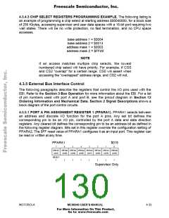
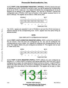
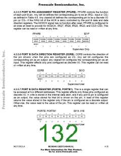
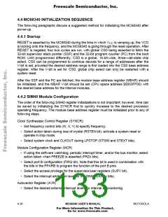
4.3.5.1 PORT A PIN ASSIGNMENT REGISTER 1 (PPARA1). PPARA1 selects between
an address and discrete I/O function for the port A pins. Any set bit defines the
corresponding pin to be an I/O pin, controlled by the port A data and data direction
registers. Any cleared bit defines the corresponding pin to be an address bit as defined in
the following register diagram. Bits set in this register override the configuration setting of
PPARA2. The $FF reset value of PPARA1 configures it as an input port. This register can
be read or written at any time.
PPARA1
$015
7
6
5
4
3
2
1
0
PRTA7 PRTA6 PRTA5 PRTA4 PRTA3 PRTA2 PRTA1 PRTA0
(A31)
(A30)
1
(A29)
1
(A28)
1
(A27)
1
(A26)
(A25)
(A24)
RESET:
1
1
1
1
Supervisor Only
MOTOROLA
MC68340 USER’S MANUAL
4- 33
For More Information On This Product,
Go to: www.freescale.com

 FREESCALE [ Freescale ]