Freescale Semiconductor, Inc.
FCM3–FCM0—Function Code Mask Bits 3–0
This field can be used to mask certain function code bits, allowing more than one
address space type to be assigned to a chip select. Any set bit masks the
corresponding function code bit.
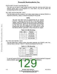
DD1, DD0—DSACK Delay Bits 1 and 0
This field determines the number of wait states added before an internal DSACK≈ is
returned for that entry. Table 4-10 lists the encoding for the DD bits.
NOTE:
The port size field must be programmed for an internal
DSACK≈ response and the FTE bit in the base address
register must be cleared for the DDx bits to have significance.
If external DSACK≈ signals are returned earlier than indicated
by the DDx bits, the cycle will terminate sooner than
programmed. See 4.2.5.2 PORT B for a discussion on using
the internal DSACK≈ generation without using the CS≈ signal.
Table 4-10. DDx Encoding
DD1
DD0
Response
0
0
Zero Wait State
One Wait State
Two Wait States
Three Wait States
0
1
1
1
0
1
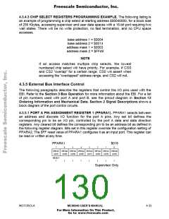
PS1, PS0—Port Size Bits 1 and 0
This field determines whether a given chip select responds with DSACK≈ and, if so,
what port size is returned. Table 4-11 lists the encoding for the PSx bits.
Table 4-11. PSx Encoding
PS1
0
PS0
0
Mode
Reserved*
0
1
16-Bit Port
1
0
8-Bit Port
1
1
External DSACK≈ Response
*Use only for 32-bit DMA transfers.
To use the external DSACK≈ response, PS1–PS0 = 11 should be selected to suppress
internal DSACK≈ generation. The DDx bits then have no significance.
4- 32
MC68340 USER’S MANUAL
MOTOROLA
For More Information On This Product,
Go to: www.freescale.com

 FREESCALE [ Freescale ]