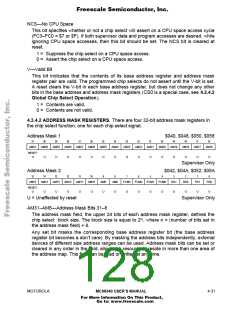
Freescale Semiconductor, Inc.
NCS—No CPU Space
This bit specifies whether or not a chip select will assert on a CPU space access cycle
(FC3–FC0 = $7 or $F). If both supervisor data and program accesses are desired, while
ignoring CPU space accesses, then this bit should be set. The NCS bit is cleared at
reset.
1 = Suppress the chip select on a CPU space access.
0 = Assert the chip select on a CPU space access.
V—Valid Bit
This bit indicates that the contents of its base address register and address mask
register pair are valid. The programmed chip selects do not assert until the V-bit is set.
A reset clears the V-bit in each base address register, but does not change any other
bits in the base address and address mask registers (CS0 is a special case, see 4.2.4.2
Global Chip Select Operation).
1 = Contents are valid.
0 = Contents are not valid.
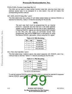
4.3.4.2 ADDRESS MASK REGISTERS. There are four 32-bit address mask registers in
the chip select function, one for each chip select signal.
Address Mask 1
$040, $048, $050, $058
31
30
29
28
27
26
25
24
23
22
21
20
19
18
17
16
AM31
AM30
AM29
AM28
AM27
AM26
AM25
AM24
AM23
AM22
AM21
AM20
AM19
AM18
AM17
AM16
RESET:
U
U
U
U
U
U
U
U
U
U
U
U
U
U
U
U
Supervisor Only
Address Mask 2
$042, $04A, $052, $05A
15
14
13
12
11
10
9
8
7
6
5
4
3
2
1
0
AM15
AM14
AM13
AM12
AM11
AM10
AM9
AM8
FCM3
FCM2
FCM1
FCM0
DD1
DD0
PS1
PS0
RESET:
U
U
U
U
U
U
U
U
U
U
U
U
U
U
U
U
U = Unaffected by reset
Supervisor Only
AM31–AM8—Address Mask Bits 31–8
The address mask field, the upper 24 bits of each address mask register, defines the
n
chip select block size. The block size is equal to 2 , where n = (number of bits set in
the address mask field) + 8.
Any set bit masks the corresponding base address register bit (the base address
register bit becomes a don’t care). By masking the address bits independently, external
devices of different size address ranges can be used. Address mask bits can be set or
cleared in any order in the field, allowing a resource to reside in more than one area of
the address map. This field can be read or written at any time.
MOTOROLA
MC68340 USER’S MANUAL
4- 31
For More Information On This Product,
Go to: www.freescale.com

 FREESCALE [ Freescale ]