Freescale Semiconductor, Inc.
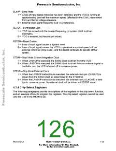
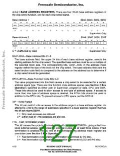
4.3.4.1 BASE ADDRESS REGISTERS. There are four 32-bit base address registers in
the chip select function, one for each chip select signal.
Base Address 1
$044, $04C, $054, $05C
31
30
29
28
27
26
25
24
23
22
21
20
19
18
17
16
BA31
BA30
BA29
BA28
BA27
BA26
BA25
BA24
BA23
BA22
BA21
BA20
BA19
BA18
BA17
BA16
RESET:
U
U
U
U
U
U
U
U
U
U
U
U
U
U
U
U
Supervisor Only
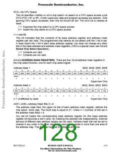
Base Address 2
$046, $04E, $056, $05E
31
30
29
28
27
26
25
24
23
22
21
20
19
18
17
16
BA15
BA14
BA13
BA12
BA11
BA10
BA9
BA8
BFC3
BFC2
BFC1
BFC0
WP
FTE
NCS
V
RESET:
U
U
U
U
U
U
U
U
U
U
U
U
U
U
0
0
U = Unaffected by reset
Supervisor Only
BA31–BA8—Base Address Bits 31–8
The base address field, the upper 24 bits of each base address register, selects the
starting address for the chip select. The specified base address must be on a multiple of
the selected block size. The corresponding bits, AM31–AM8, in the address mask
register define the size of the block for the chip select. The base address field (and the
base function code field) is compared to the address on the address bus to determine if
a chip select should be generated.
BFC3–BFC0—Base Function Code Bits 3–0
The value programmed into this field causes a chip select to be asserted for a certain
address space type. There are nine function code address spaces (see Section 3 Bus
Operation) specified as either user or supervisor, program or data, CPU, and DMA.
These bits should be used to allow access to one type of address space. If access to
more than one type of address space is desired, the FCMx bits should be used in
addition to the BFCx bits. To prevent access to CPU space, set the NCS bit.
WP—Write Protect
This bit can restrict write accesses to the address range in a base address register. An
attempt to write to the range of addresses specified in a base address register that has
this bit set returns BERR.
1 = Only read accesses are allowed.
0 = Either read or write accesses are allowed.
FTE—Fast-Termination Enable
This bit causes the cycle to terminate early with an internal DSACK≈, giving a fast two-
clock external access. When clear, all external cycles are at least three clocks. If fast
termination is enabled, the DD bits of the corresponding address mask register are
overridden (see Section 3 Bus Operation).
1 = Fast termination cycle enabled (termination determined by PS bits).
0 = Fast termination cycle disabled (termination determined by DD and PS bits).
4- 30
MC68340 USER’S MANUAL
MOTOROLA
For More Information On This Product,
Go to: www.freescale.com

 FREESCALE [ Freescale ]