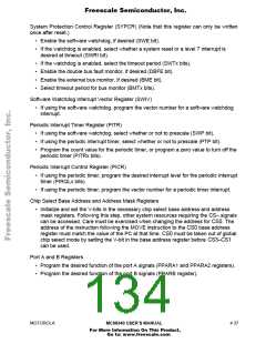
Freescale Semiconductor, Inc.
System Protection Control Register (SYPCR) (Note that this register can only be written
once after reset.)
• Enable the software watchdog, if desired (SWE bit).
• If the watchdog is enabled, select whether a system reset or a level 7 interrupt is
desired at timeout (SWRI bit).
• If the watchdog is enabled, select the timeout period (SWTx bits).
• Enable the double bus fault monitor, if desired (DBFE bit).
• Enable the external bus monitor, if desired (BME bit).
• Select timeout period for bus monitor (BMTx bits).
Software Watchdog Interrupt Vector Register (SWIV)
• If using the software watchdog, program the vector number for a software watchdog
interrupt.
Periodic Interrupt Timer Register (PITR)
• If using the software watchdog, select whether or not to prescale (SWP bit).
• If using the periodic interrupt timer, select whether or not to prescale (PTP bit).
• Program the count value for the periodic timer, or program a zero value to turn off the
periodic timer (PITRx bits).
Periodic Interrupt Control Register (PICR)
• If using the periodic timer, program the desired interrupt level for the periodic interrupt
timer (PIRQLx bits).
• If using the periodic timer, program the vector number for a periodic timer interrupt.
Chip Select Base Address and Address Mask Registers
• Initialize and set the V-bits in the necessary chip select base address and address
mask registers. Following this step, other system resources requiring the CS≈ signals
can be accessed. Care must be exercised when changing the address for CS0. The
address of the instruction following the MOVE instruction to the CS0 base address
register must match the value of the PC at that time. CS0 must be taken out of global
chip select mode by setting the V-bit in the base address register before CS3–CS1
can be used.
Port A and B Registers
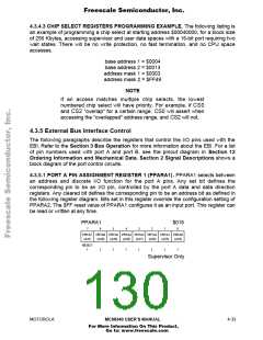
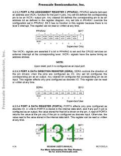
• Program the desired function of the port A signals (PPARA1 and PPARA2 registers).
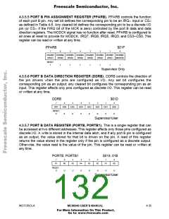
• Program the desired function of the port B signals (PPARB register).
MOTOROLA
MC68340 USER’S MANUAL
4- 37
For More Information On This Product,
Go to: www.freescale.com

 FREESCALE [ Freescale ]