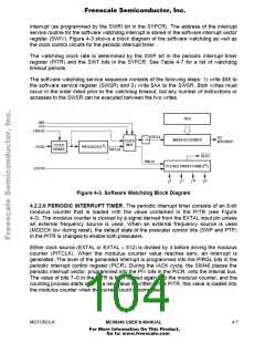
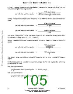
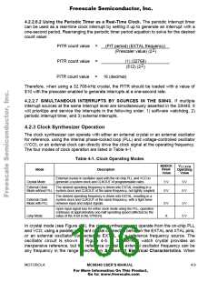
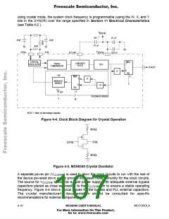
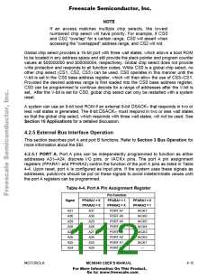
Freescale Semiconductor, Inc.
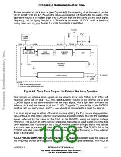
To use an external clock source (see Figure 4-6), the operating clock frequency can be
driven directly into the EXTAL pin (the XTAL pin must be left floating for this case). This
approach results in a system clock and CLKOUT that are the same as the input signal
frequency, but not tightly coupled to it. To enable this mode, MODCK must be held low
during reset, and V
held at 0 V while the chip is in operation.
CCSYN
V
CCSYN
1
XFC
0.1 µF
.01 µF
EXTERNAL
CLOCK
V
CCSYN
EXTAL
XTAL
XFC PIN
CRYSTAL
OSCILLATOR
PHASE
COMPARATOR
LOW-PASS
FILTER
VCO
FEEDBACK
DIVIDER
2
CLKOUT
CLOCK CONTROL
SYSTEM
CLOCK
NOTES:
1. Must be low-leakage capacitor.
2. External mode uses this path only.
Figure 4-6. Clock Block Diagram for External Oscillator Operation
Alternatively, an external clock signal can be directly driven into EXTAL (with XTAL left
floating) using the on-chip PLL. This configuration results in an internal clock and
CLKOUT signal of the same frequency as the input signal, with a tight skew between the
external clock and the internal clock and CLKOUT signals. To enable this mode, MODCK
must be held low during reset, and V
should be connected to a quiet 5-V source.
CCSYN
If an input signal loss for either of the clock modes utilizing the PLL occurs, chip operation
can continue in limp mode with the VCO running at approximately one-half the operating
speed (affected by the value of the X-bit in the SYNCR), using an internal voltage
reference. The SLIMP bit in the SYNCR indicates that a loss of input signal reference has
been detected. The RSTEN bit in the SYNCR controls whether an input signal loss causes
a system reset or causes the device to operate in limp mode. The SLOCK bit in the
SYNCR indicates when the VCO has locked onto the desired frequency or if an external
clock is being used.
4.2.3.1 PHASE COMPARATOR AND FILTER. The phase comparator takes the output of
the frequency divider and compares it to an external input signal reference. The result of
MOTOROLA
MC68340 USER’S MANUAL
4- 11
For More Information On This Product,
Go to: www.freescale.com

 FREESCALE [ Freescale ]