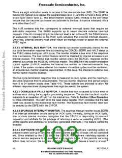
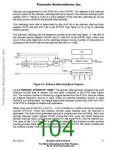
Freescale Semiconductor, Inc.
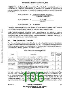
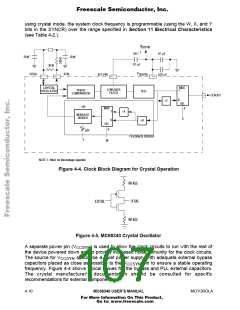
using crystal mode, the system clock frequency is programmable (using the W, X, and Y
bits in the SYNCR) over the range specified in Section 11 Electrical Characteristics
(see Table 4-2.).
V
DDSYN
1
XFC
0.1 µF
20 pF
20 pF
0.1 µF
20 M
V
EXTAL
XTAL
XFC PIN
DDSYN
0.01 µF
CRYSTAL
OSCILLATOR
MUX
1
LOW-PASS
FILTER
PHASE
COMPARATOR
VCO
CLKOUT
0
÷2
SEL
÷64
MUX
0
1
÷4
MODULUS
DIVIDER
X
0
÷8
SEL
6
0
$3F
FEEDBACK DIVIDER
Y
W
NOTE 1: Must be low-leakage capacitor.
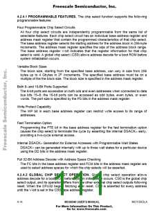
Figure 4-4. Clock Block Diagram for Crystal Operation
60 kΩ
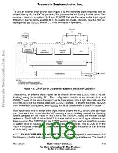
XTAL
EXTAL
.
60 kΩ
Figure 4-5. MC68340 Crystal Oscillator
A separate power pin (V ) is used to allow the clock circuits to run with the rest of
CCSYN
the device powered down and to provide increased noise immunity for the clock circuits.
The source for V should be a quiet power supply with adequate external bypass
CCSYN
capacitors placed as close as possible to the V
pin to ensure a stable operating
CCSYN
frequency. Figure 4-4 shows typical values for the bypass and PLL external capacitors.
The crystal manufacturer's documentation should be consulted for specific
recommendations for external components.
4- 10
MC68340 USER’S MANUAL
MOTOROLA
For More Information On This Product,
Go to: www.freescale.com

 FREESCALE [ Freescale ]