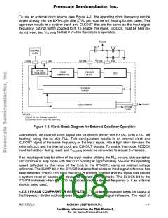
Freescale Semiconductor, Inc.
NOTE
If an access matches multiple chip selects, the lowest
numbered chip select will have priority. For example, if CS0
and CS2 "overlap" for a certain range, CS0 will assert when
accessing the "overlapped" address range, and CS2 will not.
Global chip select provides a 16-bit port with three wait states, which allows a boot ROM
to be located in any address space and still provide the stack pointer and program counter
values at $00000000 and $00000004, respectively. Global chip select does not provide
write protection and responds to all function codes. While CS0 is a global chip select, no
other chip select (CS1, CS2, CS3) can be used. CS0 operates in this manner until the
V-bit is set in the CS0 base address register, which will then allow the use of CS3–CS1.
Provided the desired address range is first loaded into the CS0 base address register,
CS0 can be programmed to continue decode for a range of addresses after the V-bit is
set, After the V-bit is set for CS0, global chip select can only be restarted with a system
reset.
A system can use an 8-bit boot ROM if an external 8-bit DSACK≈ that responds in two or
less wait states is generated. The 8-bit DSACK≈ must respond in two or less wait states
so that the global chip select, which responds with three wait states, will not be used. See
Section 10 Applications for a detailed discussion.
4.2.5 External Bus Interface Operation
This section describes port A and port B functions. Refer to Section 3 Bus Operation for
more information about the EBI.
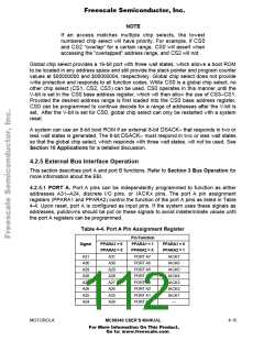
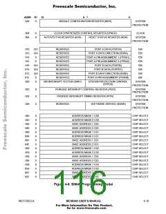
4.2.5.1 PORT A. Port A pins can be independently programmed to function as either
addresses A31–A24, discrete I/O pins, or IACKx pins. The port A pin assignment
registers (PPARA1 and PPARA2) control the function of the port A pins as listed in Table
4-4. Upon reset, port A is configured as input pins. If the system uses these signals as
addresses, pulldowns should be put on these signals to avoid indeterminate values until
the port A registers can be programmed.
Table 4-4. Port A Pin Assignment Register
Pin Function
Signal
PPARA1 = 0
PPARA2 = 0
A31
PPARA1 = 1
PPARA2 = X
PORT A7
PORT A6
PORT A5
PORT A4
PORT A3
PORT A2
PORT A1
PORT A0
PPARA1 = 0
PPARA2 = 1
IACK7
A31
A30
A29
A28
A27
A26
A25
A24
A30
IACK6
A29
IACK5
A28
IACK4
A27
IACK3
A26
IACK2
A25
IACK1
A24
—
MOTOROLA
MC68340 USER’S MANUAL
4- 15
For More Information On This Product,
Go to: www.freescale.com

 FREESCALE [ Freescale ]