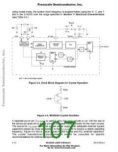
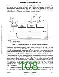
Freescale Semiconductor, Inc.
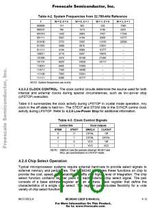
4.2.4.1 PROGRAMMABLE FEATURES. The chip select function supports the following
programmable features:
Four Programmable Chip Select Circuits
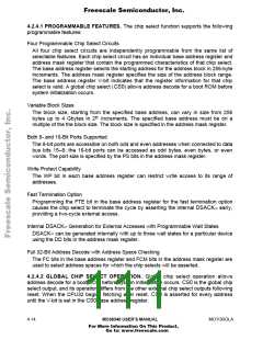
All four chip select circuits are independently programmable from the same list of
selectable features. Each chip select circuit has an individual base address register and
address mask register that contain the programmed characteristics of that chip select.
The base address register selects the starting address for the address block in 256-byte
increments. The address mask register specifies the size of the address block range.
The base address register V-bit indicates that the register information for that chip
select is valid. A global chip select (CS0) allows address decode for a boot ROM before
system initialization occurs.
Variable Block Sizes
The block size, starting from the specified base address, can vary in size from 256
n
bytes up to 4 Gbytes in 2 increments. The specified base address must be on a
multiple of the the block size. The block size is specified in the address mask register.
Both 8- and 16-Bit Ports Supported
The 8-bit ports are accessible on both odd and even addresses when connected to data
bus bits 15–8; the 16-bit ports can be accessed as odd bytes, even bytes, or even
words. The port size is specified by the PS bits in the address mask register.
Write Protect Capability
The WP bit in each base address register can restrict write access to its range of
addresses.
Fast Termination Option
Programming the FTE bit in the base address register for the fast termination option
causes the chip select to terminate the cycle by asserting the internal DSACK≈ early,
providing a two-cycle external access.
Internal DSACK≈ Generation for External Accesses with Programmable Wait States
DSACK≈ can be generated internally with up to three wait states for a particular device
using the DD bits in the address mask register.
Full 32-Bit Address Decode with Address Space Checking
The FC bits in the base address register and FCM bits in the address mask register are
used to select address spaces for which the chip selects will be asserted.
4.2.4.2 GLOBAL CHIP SELECT OPERATION. Global chip select operation allows
address decode for a boot ROM before system initialization occurs. CS0 is the global chip
select output, and its operation differs from the other external chip select outputs following
reset. When the CPU32 begins fetching after reset, CS0 is asserted for every address
until the V-bit is set in the CS0 base address register.
4- 14
MC68340 USER’S MANUAL
MOTOROLA
For More Information On This Product,
Go to: www.freescale.com

 FREESCALE [ Freescale ]