Freescale Semiconductor, Inc.
MSCAN Controller
Programmer’s Model of Control Registers
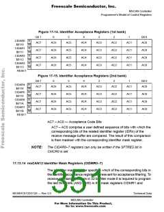
Figure 17-14. Identifier Acceptance Registers (1st bank)
Bit 7
6
5
4
3
2
1
Bit 0
AC0
CIDAR0
$0110
R
W
R
AC7
AC6
AC5
AC4
AC3
AC2
AC1
CIDAR1
$0111
AC7
AC7
AC6
AC6
AC5
AC5
AC4
AC4
AC3
AC3
AC2
AC2
AC1
AC1
AC0
AC0
W
R
CIDAR2
$0112
W
R
CIDAR3
$0113
AC7
-
AC6
-
AC5
-
AC4
-
AC3
-
AC2
-
AC1
-
AC0
-
W
RESET
Figure 17-15. Identifier Acceptance Registers (2nd bank)
Bit 7
6
5
4
3
2
1
Bit 0
AC0
CIDAR4
$0118
R
W
R
AC7
AC6
AC5
AC4
AC3
AC2
AC1
CIDAR5
$0119
AC7
AC7
AC6
AC6
AC5
AC5
AC4
AC4
AC3
AC3
AC2
AC2
AC1
AC1
AC0
AC0
W
R
CIDAR6
$011A
W
R
CIDAR7
$011B
AC7
-
AC6
-
AC5
-
AC4
-
AC3
-
AC2
-
AC1
-
AC0
-
W
RESET
AC7 – AC0 — Acceptance Code Bits
AC7 – AC0 comprise a user defined sequence of bits with which the
corresponding bits of the related identifier register (IDRn) of the
receive message buffer are compared. The result of this comparison
is then masked with the corresponding identifier mask register.
NOTE: The CIDAR0–7 registers can only be written if the SFTRES bit in
CMCR0 is set.
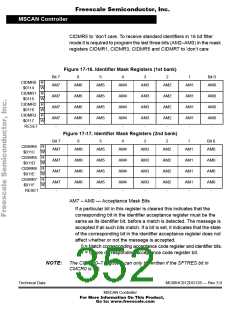
17.13.14 msCAN12 Identifier Mask Registers (CIDMR0–7)
The identifier mask register specifies which of the corresponding bits in
the identifier acceptance register are relevant for acceptance filtering. To
receive standard identifiers in 32 bit filter mode it is required to program
the last three bits (AM2–AM0) in the mask registers CIDMR1 and
MC68HC912DG128 — Rev 3.0
Technical Data
MSCAN Controller
For More Information On This Product,
Go to: www.freescale.com

 FREESCALE [ Freescale ]