Freescale Semiconductor, Inc.
Clock Functions
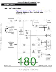
Clock Divider Chains
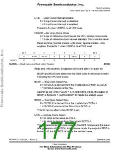
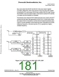
Bus clock select bits BCSP and BCSS in the clock select register
(CLKSEL) determine which clock drives SYSCLK for the main system
including the CPU and buses. BCSS has no effect if BCSP is set. During
the transition, the clock select output will be held low and all CPU activity
will cease until the transition is complete.
The Module Clock Select bit MCS determines the clock used by the ECT
module and the baud rate generators of the SCIs. In limp-home mode,
the output of MCS is forced to 0, but the MCS bit reads the latched value.
It allows normal operation of the serial and timer subsystems at a fixed
reference frequency while allowing the CPU to operate at a higher,
variable frequency.
XCLK
÷ 2048
÷4
0:0:0
0:0:0
REGISTER: COPCTL
BITS: CR2, CR1, CR0
REGISTER: RTICTL
BITS: RTR2, RTR1, RTR0
REGISTER: RTICTL
BIT:RTBYP
0:0:1
0:1:0
0:0:1
0:1:0
÷ 2
÷ 4
÷ 4
÷ 4
÷ 4
÷ 2
÷ 2
SC0BD
MODULUS DIVIDER:
÷ 1, 2, 3, 4, 5, 6,...,8190, 8191
SCI0
÷ 2
0:1:1
1:0:0
1:0:1
1:1:0
1:1:1
0:1:1
1:0:0
1:0:1
1:1:0
1:1:1
MCLK
RECEIVE
BAUD RATE (16x)
÷ 2
÷ 2
÷ 2
÷ 2
÷ 16
SCI0
TRANSMIT
BAUD RATE (1x)
SC1BD
MODULUS DIVIDER:
÷ 1, 2, 3, 4, 5, 6,...,8190, 8191
SCI1
RECEIVE
BAUD RATE (16x)
÷ 16
SCI1
TRANSMIT
BAUD RATE (1x)
TO RTI
TO COP
Figure 11-7. Clock Chain for SCI0, SCI1, RTI, COP
MC68HC912DG128 — Rev 3.0
Technical Data
Clock Functions
For More Information On This Product,
Go to: www.freescale.com

 FREESCALE [ Freescale ]