Freescale Semiconductor, Inc.
Timer Interface Module (TIM)
I/O Registers
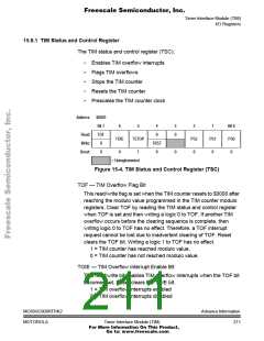
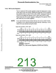
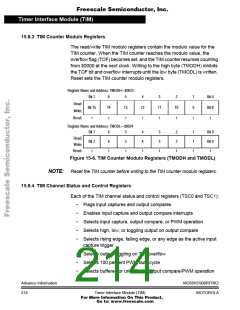
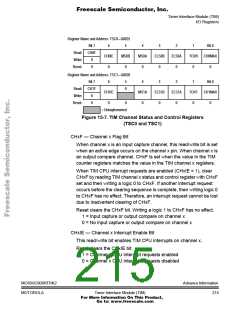
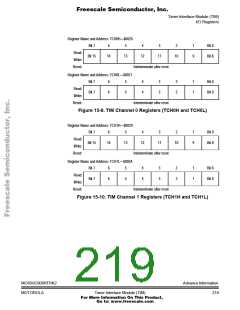
Register Name and Address: TSC0—$0025
Bit 7
6
CH0IE
0
5
MS0B
0
4
MS0A
0
3
ELS0B
0
2
ELS0A
0
1
Bit 0
Read: CH0F
TOV0 CH0MAX
Write:
Reset:
0
0
0
1
0
Register Name and Address: TSC1—$0028
Bit 7
6
CH1IE
0
5
0
4
MS1A
0
3
ELS1B
0
2
ELS1A
0
Bit 0
Read: CH1F
TOV1 CH1MAX
Write:
Reset:
0
0
0
0
0
= Unimplemented
Figure 15-7. TIM Channel Status and Control Registers
(TSC0 and TSC1)
CHxF — Channel x Flag Bit
When channel x is an input capture channel, this read/write bit is set
when an active edge occurs on the channel x pin. When channel x is
an output compare channel, CHxF is set when the value in the TIM
counter registers matches the value in the TIM channel x registers.
When TIM CPU interrupt requests are enabled (CHxIE = 1), clear
CHxF by reading TIM channel x status and control register with CHxF
set and then writing a logic 0 to CHxF. If another interrupt request
occurs before the clearing sequence is complete, then writing logic 0
to CHxF has no effect. Therefore, an interrupt request cannot be lost
due to inadvertent clearing of CHxF.
Reset clears the CHxF bit. Writing a logic 1 to CHxF has no effect.
1 = Input capture or output compare on channel x
0 = No input capture or output compare on channel x
CHxIE — Channel x Interrupt Enable Bit
This read/write bit enables TIM CPU interrupts on channel x.
Reset clears the CHxIE bit.
1 = Channel x CPU interrupt requests enabled
0 = Channel x CPU interrupt requests disabled
MC68HC908RFRK2
MOTOROLA
AdvanceInformation
Timer Interface Module (TIM)
215
For More Information On This Product,
Go to: www.freescale.com

 FREESCALE [ Freescale ]