Freescale Semiconductor, Inc.
Timer Interface Module (TIM)
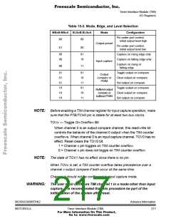
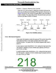
CHxMAX — Channel x Maximum Duty Cycle Bit
When the TOVx bit is at logic 0, setting the CHxMAX bit forces the
duty cycle of buffered and unbuffered PWM signals to 100 percent. As
Figure 15-8 shows, the CHxMAX bit takes effect in the cycle after it
is set or cleared. The output stays at the 100 percent duty cycle level
until the cycle after CHxMAX is cleared.
OVERFLOW
OVERFLOW
OVERFLOW
OVERFLOW
OVERFLOW
PERIOD
PTBx/TCHx
CHxMAX
OUTPUT
COMPARE
OUTPUT
COMPARE
OUTPUT
COMPARE
OUTPUT
COMPARE
Figure 15-8. CHxMAX Latency
15.9.5 TIM Channel Registers
These read/write registers contain the captured TIM counter value of the
input capture function or the output compare value of the output
compare function. The state of the TIM channel registers after reset is
unknown.
In input capture mode (MSxB:MSxA = 0:0), reading the high byte of the
TIM channel x registers (TCHxH) inhibits input captures until the low
byte (TCHxL) is read.
In output compare mode (MSxB:MSxA ≠ 0:0), writing to the high byte of
the TIM channel x registers (TCHxH) inhibits output compares until the
low byte (TCHxL) is written.
Advance Information
218
MC68HC908RFRK2
Timer Interface Module (TIM)
MOTOROLA
For More Information On This Product,
Go to: www.freescale.com

 FREESCALE [ Freescale ]