Introduction
Part 3 On-Chip Clock Synthesis (OCCS)
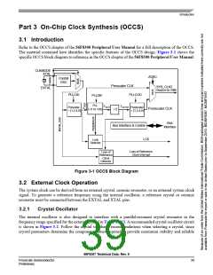
3.1 Introduction
Refer to the OCCS chapter of the 56F8300 Peripheral User Manual for a full description of the OCCS.
The material contained here identifies the specific features of the OCCS design. Figure 3-1 shows the
specific OCCS block diagram to reference in the OCCS chapter of the 56F8300 Peripheral User Manual.
CLKMODE
XTAL
ZSRC
Crystal
OSC
Prescaler CLK
PLLCOD
SYS_CLK2
Source to SIM
EXTAL
PLLCID
PLLDB
PLL
FOUT
FOUT/2
Postscaler
Prescaler
÷ (1,2,4,8)
Postscaler CLK
÷2
x (1 to 128)
÷ (1,2,4,8)
Bus
Interface
Bus Interface & Control
LCK
Lock
Detector
Loss of Reference
Clock Interrupt
Loss of
Reference
Clock
Detector
Figure 3-1 OCCS Block Diagram
3.2 External Clock Operation
The system clock can be derived from an external crystal, ceramic resonator, or an external system clock
signal. To generate a reference frequency using the internal oscillator, a reference crystal or ceramic
resonator must be connected between the EXTAL and XTAL pins.
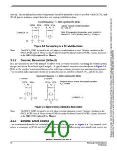
3.2.1
Crystal Oscillator
The internal oscillator is also designed to interface with a parallel-resonant crystal resonator in the
frequency range specified for the external crystal in Table 10-13. A recommended crystal oscillator circuit
is shown in Figure 3-2. Follow the crystal supplier’s recommendations when selecting a crystal, since
crystal parameters determine the component values required to provide maximum stability and reliable
56F8367 Technical Data, Rev. 9
Freescale Semiconductor
Preliminary
39

 FREESCALE [ Freescale ]