Signal Pins
Table 2-2 Signal and Package Information for the 160-Pin LQFP and MBGA (Continued)
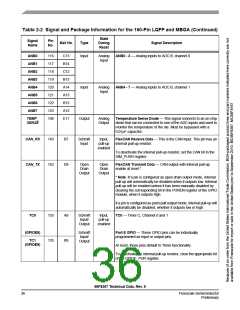
State
During
Reset
Signal
Name
Pin
No.
Ball No.
Type
Signal Description
TD0
129
B10
Schmitt
Input/
Output
Input,
pull-up
enabled
TD0 - 3— Timer D, Channels 0, 1, 2 and 3
(GPIOE10)
Schmitt
Input/
Output
Port E GPIO — These GPIO pins can be individually
programmed as input or output pins.
TD1
(GPIOE11)
130
131
132
A10
D10
E10
At reset, these pins default to Timer functionality.
TD2
(GPIOE12)
To deactivate the internal pull-up resistor, clear the appropriate bit
of the GPIOE_PUR register. See Part 6.5.6 for details.
TD3
(GPIOE13)
IRQA
IRQB
65
66
K9
P9
Schmitt
Input
Input,
pull-up
enabled
External Interrupt Request A and B — The IRQA and IRQB
inputs are asynchronous external interrupt requests during Stop
and Wait mode operation. During other operating modes, they are
synchronized external interrupt requests, which indicate an
external device is requesting service. They can be programmed to
be level-sensitive or negative-edge triggered.
To deactivate the internal pull-up resistor, set the IRQ bit in the
SIM_PUDR register. See Part 6.5.6 for details.
RESET
98
J14
Schmitt
Input
Input,
pull-up
enabled
Reset — This input is a direct hardware reset on the processor.
When RESET is asserted low, the device is initialized and placed
in the reset state. A Schmitt trigger input is used for noise
immunity. When the RESET pin is deasserted, the initial chip
operating mode is latched from the EXTBOOT pin. The internal
reset signal will be deasserted synchronous with the internal
clocks after a fixed number of internal clocks.
To ensure complete hardware reset, RESET and TRST should be
asserted together. The only exception occurs in a debugging
environment when a hardware device reset is required and the
JTAG/EOnCE module must not be reset. In this case, assert
RESET but do not assert TRST.
Note: The internal Power-On Reset will assert on initial power-up.
To deactivate the internal pull-up resistor, set the RESET bit in the
SIM_PUDR register. See Part 6.5.6 for details.
RSTO
97
J13
Output
Output
Reset Output — This output reflects the internal reset state of the
chip.
56F8367 Technical Data, Rev. 9
Freescale Semiconductor
Preliminary
37

 FREESCALE [ Freescale ]