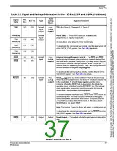
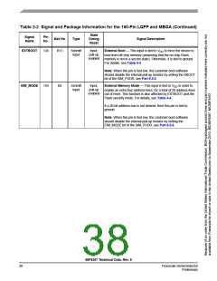
Registers
the OCCS_COHL bit high as well.
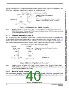
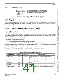
Note: When using an external clocking source with
this configuration, the input “CLKMODE” should be
high and the COHL bit in the OSCTL register
should be set to 1.
XTAL
EXTAL
V
External
Clock
SS
Figure 3-4 Connecting an External Clock Register
3.3 Registers
When referring to the register definitions for the OCCS in the 56F8300 Peripheral User Manual, use the
register definitions without the internal Relaxation Oscillator, since the 56F8367/56F8167 do NOT
contain this oscillator.
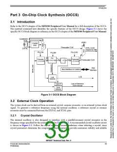
Part 4 Memory Operating Modes (MEM)
4.1 Introduction
The 56F8367 and 56F8167 devices are 16-bit motor-control chips based on the 56800E core. These parts
use a Harvard-style architecture with two independent memory spaces for Data and Program. On-chip
RAM and Flash memory are used in both spaces.
This chapter provides memory maps for:
•
•
Program Address Space including the Interrupt Vector Table
Data Address Space including the EOnCE Memory and Peripheral Memory Maps
On-chip memory sizes for each device are summarized in Table 4-1. Flash memories’ restrictions are
identified in the “Use Restrictions” column of Table 4-1.
Note: Data Flash and Program RAM are NOT available on the 56F8167 device.
Table 4-1 Chip Memory Configurations
On-Chip Memory
56F8367
56F8167
Use Restrictions
Program Flash
512KB
512KB
Erase/Program via Flash interface unit and word writes to
CDBW
Data Flash
32KB
—
Erase/Program via Flash interface unit and word writes to
CDBW. Data Flash can be read via one of CDBR or XDB2, but
not both simultaneously
Program RAM
Data RAM
4KB
32KB
32KB
—
None
32KB
32KB
None
Program Boot Flash
Erase/Program via Flash Interface unit and word to CDWB
56F8367 Technical Data, Rev. 9
Freescale Semiconductor
Preliminary
41

 FREESCALE [ Freescale ]