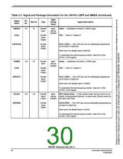
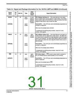
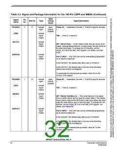
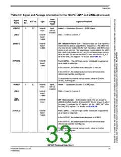
Table 2-2 Signal and Package Information for the 160-Pin LQFP and MBGA (Continued)
State
During
Reset
Signal
Name
Pin
No.
Ball No.
Type
Signal Description
PWMA0
PWMA1
PWMA2
PWMA3
PWMA4
PWMA5
ISA0
73
75
M11
P12
N11
M12
P13
N12
A11
Output
In reset, PWMA0 - 5 — These are six PWMA outputs.
output is
disabled,
pull-up is
enabled
76
78
79
81
126
Schmitt
Input
Input,
pull-up
enabled
ISA0 - 2 — These three input current status pins are used for
top/bottom pulse width correction in complementary channel
operation for PWMA.
(GPIOC8)
Schmitt
Input/
Output
Port C GPIO — These GPIO pins can be individually
programmed as input or output pins.
ISA1
(GPIOC9)
127
128
C11
D11
In the 56F8367, these pins default to ISA functionality after reset.
ISA2
(GPIOC10)
In the 56F8167, the default state is not one of the functions
offered and must be reconfigured.
To deactivate the internal pull-up resistor, clear the appropriate bit
of the GPIOC_PUR register. For details, see Part 6.5.8.
FAULTA0
FAULTA1
FAULTA2
82
84
85
N13
N14
M13
Schmitt
Input
Input,
pull-up
enabled
FAULTA0 - 2 — These three fault input pins are used for
disabling selected PWMA outputs in cases where fault conditions
originate off-chip.
To deactivate the internal pull-up resistor, set the PWMA0 bit in
the SIM_PUDR register. For details, see Part 6.5.8.
FAULTA3
87
M14
Schmitt
Input
Input,
pull-up
enabled
FAULTA3 — This fault input pin is used for disabling selected
PWMA outputs in cases where fault conditions originate off-chip.
To deactivate the internal pull-up resistor, set the PWMA1 bit in
the SIM_PUDR register. See Part 6.5.6 for details.
PWMB0
PWMB1
PWMB2
PWMB3
PWMB4
PWMB5
38
39
40
43
44
45
N1
P1
N2
N3
P2
M3
Output
In reset, PWMB0 - 5 — Six PWMB output pins.
output is
disabled,
pull-up is
enabled
56F8367 Technical Data, Rev. 9
34
Freescale Semiconductor
Preliminary

 FREESCALE [ Freescale ]