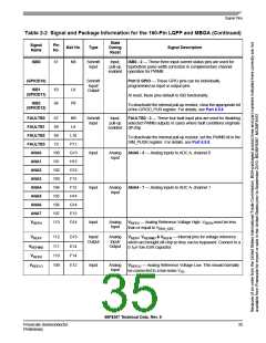
Signal Pins
Table 2-2 Signal and Package Information for the 160-Pin LQFP and MBGA (Continued)
State
During
Reset
Signal
Name
Pin
No.
Ball No.
Type
Signal Description
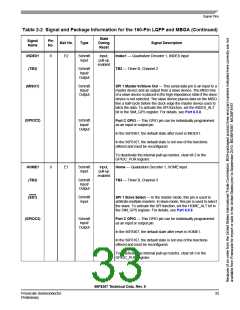
MOSI0
148
B6
Input/
Output
In reset, SPI 0 Master Out/Slave In — This serial data pin is an output
output is from a master device and an input to a slave device. The master
disabled, device places data on the MOSI line a half-cycle before the clock
pull-up is edge the slave device uses to latch the data.
enabled
(GPIOE5)
Input/
Output
Port E GPIO — This GPIO pin can be individually programmed as
an input or output pin.
After reset, the default state is MOSI0.
To deactivate the internal pull-up resistor, clear bit 5 in the
GPIOE_PUR register.
MISO0
147
D4
Input/
Output
Input,
pull-up
enabled
SPI 0 Master In/Slave Out — This serial data pin is an input to a
master device and an output from a slave device. The MISO line
of a slave device is placed in the high-impedance state if the slave
device is not selected. The slave device places data on the MISO
line a half-cycle before the clock edge the master device uses to
latch the data.
(GPIOE6)
Input/
Port E GPIO — This GPIO pin can be individually programmed as
Output
an input or output pin.
After reset, the default state is MISO0.
To deactivate the internal pull-up resistor, clear bit 6 in the
GPIOE_PUR register.
SS0
145
D5
Input
Input,
pull-up
enabled
SPI 0 Slave Select — SS0 is used in slave mode to indicate to
the SPI module that the current transfer is to be received.
(GPIOE7)
Input/
Port E GPIO — This GPIO pin can be individually programmed as
Output
input or output pin.
After reset, the default state is SS0.
To deactivate the internal pull-up resistor, clear bit 7 in the
GPIOE_PUR register.
56F8367 Technical Data, Rev. 9
Freescale Semiconductor
Preliminary
31

 FREESCALE [ Freescale ]