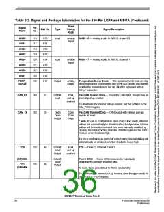
Table 2-2 Signal and Package Information for the 160-Pin LQFP and MBGA (Continued)
State
During
Reset
Signal
Name
Pin
No.
Ball No.
Type
Signal Description
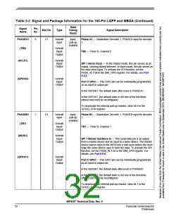
PHASEA1
(TB0)
6
C1
Schmitt
Input
Input,
pull-up
enabled
Phase A1 — Quadrature Decoder 1, PHASEA input for decoder
1.
Schmitt
Input/
TB0 — Timer B, Channel 0
Output
(SCLK1)
Schmitt
Input/
SPI 1 Serial Clock — In the master mode, this pin serves as an
output, clocking slaved listeners. In slave mode, this pin serves as
the data clock input. To activate the SPI function, set the
PHSA_ALT bit in the SIM_GPS register. For details, see Part
6.5.8.
Output
(GPIOC0)
Schmitt
Input/
Port C GPIO — This GPIO pin can be individually programmed
Output
as an input or output pin.
In the 56F8367, the default state after reset is PHASEA1.
In the 56F8167, the default state is not one of the functions
offered and must be reconfigured.
To deactivate the internal pull-up resistor, clear bit 0 in the
GPIOC_PUR register.
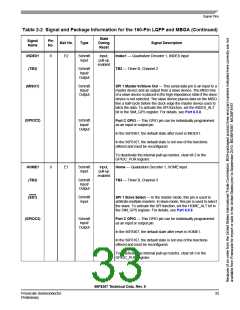
PHASEB1
(TB1)
7
D1
Schmitt
Input
Input,
pull-up
enabled
Phase B1 — Quadrature Decoder 1, PHASEB input for decoder
1.
Schmitt
Input/
TB1 — Timer B, Channel 1
Output
(MOSI1)
Schmitt
Input/
SPI 1 Master Out/Slave In — This serial data pin is an output
from a master device and an input to a slave device. The master
device places data on the MOSI line a half-cycle before the clock
edge the slave device uses to latch the data. To activate the SPI
function, set the PHSB_ALT bit in the SIM_GPS register. For
details, see Part 6.5.8.
Output
(GPIOC1)
Schmitt
Input/
Port C GPIO — This GPIO pin can be individually programmed
Output
as an input or output pin.
In the 56F8367, the default state after reset is PHASEB1.
In the 56F8167, the default state is not one of the functions
offered and must be reconfigured.
To deactivate the internal pull-up resistor, clear bit 1 in the
GPIOC_PUR register.
56F8367 Technical Data, Rev. 9
32
Freescale Semiconductor
Preliminary

 FREESCALE [ Freescale ]