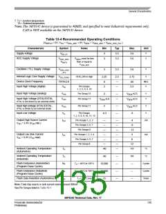
10.2 DC Electrical Characteristics
Note: The 56F8145 device is specified to meet Industrial requirements only; CAN is NOT available on the
56F8145 device.
Table 10-5 DC Electrical Characteristics
At Recommended Operating Conditions; see Table 10-4
Characteristic
Output High Voltage
Output Low Voltage
Symbol
Notes
Min
2.4
—
Typ
—
—
0
Max
—
Unit
V
Test Conditions
IOH = IOHmax
V
OH
V
IOL = IOLmax
V
0.4
OL
Pin Groups
1, 2, 5, 6, 9
VIN = 3.0V to 5.5V
I
Digital Input Current High
pull-up enabled or disabled
—
+/- 2.5
μA
IH
Pin Group 10
VIN = 3.0V to 5.5V
I
Digital Input Current High
with pull-down
40
80
160
μA
IH
Pin Group 13
Pin Group 12
VIN = VDDA
VIN = VDDA
VIN = 0V
I
Analog Input Current High
ADC Input Current High
—
—
0
0
+/- 2.5
+/- 3.5
-50
μA
μA
μA
IHA
I
IHADC
Pin Groups
1, 2, 5, 6, 9
I
Digital Input Current Low
pull-up enabled
-200
-100
IL
Pin Groups
1, 2, 5, 6, 9
VIN = 0V
VIN = 0V
I
Digital Input Current Low
pull-up disabled
—
—
0
0
+/- 2.5
+/- 2.5
μA
μA
IL
Pin Group 10
I
Digital Input Current Low
with pull-down
IL
Pin Group 13
Pin Group 12
VIN = 0V
VIN = 0V
I
Analog Input Current Low
ADC Input Current Low
—
—
—
0
0
0
+/- 2.5
+/- 3.5
+/- 2.5
μA
μA
μA
ILA
I
ILADC
VIN = VDD or 0V
I
EXTAL Input Current Low
clock input
EXTAL
CLKMODE = High
CLKMODE = Low
VIN = VDDA or 0V
VIN = VDDA or 0V
I
XTAL Input Current Low
clock input
—
—
—
0
—
0
+/- 2.5
200
μA
μA
μA
XTAL
Pin Groups
1, 2, 3, 4, 5, 6, 7, 8
VOUT = 3.0V to 5.5V or 0V
I
Output Current
High Impedance State
+/- 2.5
OZ
Pin Groups
2, 6, 9,10
V
V
Schmitt Trigger Input
Hysteresis
—
—
—
0.3
4.5
5.5
—
—
—
—
—
—
HYS
pF
pF
C
Input Capacitance
(EXTAL/XTAL)
INC
C
Output Capacitance
(EXTAL/XTAL)
OUTC
pF
pF
C
Input Capacitance
Output Capacitance
—
—
6
6
—
—
—
—
IN
C
OUT
See Pin Groups listed in Table 10-1
(VREFH - VREFLO) X 1
=
RES
212
m
56F8345 Technical Data, Rev. 17
136
Freescale Semiconductor
Preliminary

 FREESCALE [ Freescale ]