of devices designed for 3.3V and 5V power supplies. In such systems, a bus may carry both 3.3V- and
5V-compatible I/O voltage levels (a standard 3.3V I/O is designed to receive a maximum voltage of 3.3V
± 10% during normal operation without causing damage). This 5V-tolerant capability therefore offers the
power savings of 3.3V I/O levels combined with the ability to receive 5V levels without damage.
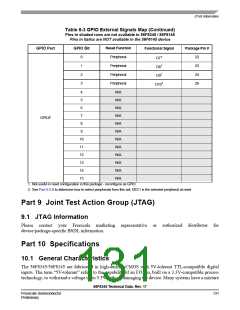
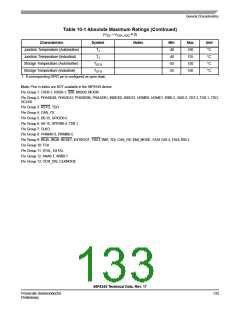
Absolute maximum ratings in Table 10-1 are stress ratings only, and functional operation at the maximum
is not guaranteed. Stress beyond these ratings may affect device reliability or cause permanent damage to
the device.
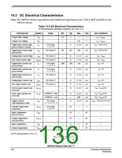
Note: All specifications meet both Automotive and Industrial requirements unless individual
specifications are listed.
Note: The 56F8145 device is guaranteed to 40MHz and specified to meet Industrial requirements only.
CAUTION
This device contains protective circuitry to guard against damage
due to high static voltage or electrical fields. However, normal
precautions are advised to avoid application of any voltages higher
than maximum-rated voltages to this high-impedance circuit.
Reliability of operation is enhanced if unused inputs are tied to an
appropriate voltage level.
Note: The 56F8145 device is specified to meet Industrial requirements only; CAN is NOT available on the
56F8145 device.
Table 10-1 Absolute Maximum Ratings
(VSS = VSSA_ADC = 0)
Characteristic
Supply voltage
Symbol
Notes
Min
- 0.3
- 0.3
Max
4.0
Unit
V
VDD_IO
ADC Supply Voltage
VDDA_ADC,
VREFH
VREFH must be less than or
equal to VDDA_ADC
4.0
V
Oscillator / PLL Supply Voltage
Internal Logic Core Supply Voltage
Input Voltage (digital)
VDDA_OSC_PLL
VDD_CORE
VIN
- 0.3
- 0.3
-0.3
-0.3
-0.3
4.0
3.0
6.0
4.0
V
V
V
V
V
OCR_DIS is High
Pin Groups 1, 2, 5, 6, 9, 10
Pin Groups 11, 12, 13
Input Voltage (analog)
VINA
Pin Groups 1, 2, 3, 4, 5, 6, 7, 8
Output Voltage
VOUT
4.0
6.01
Pin Group 4
Output Voltage (open drain)
VOD
TA
-0.3
-40
-40
6.0
125
105
V
Ambient Temperature (Automotive)
Ambient Temperature (Industrial)
°C
°C
TA
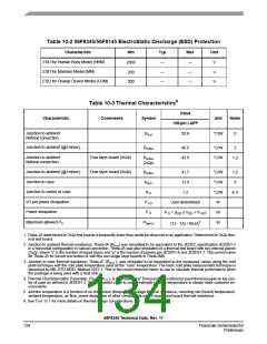
56F8345 Technical Data, Rev. 17
132
Freescale Semiconductor
Preliminary

 FREESCALE [ Freescale ]