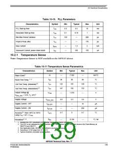
General Characteristics
7. TJ = Junction temperature
TA = Ambient temperature
Note: The 56F8145 device is guaranteed to 40MHz and specified to meet Industrial requirements only;
CAN is NOT available on the 56F8145 device.
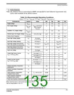
Table 10-4 Recommended Operating Conditions
(VREFLO = 0V, VSS = VSSA_ADC = 0V, VDDA = VDDA_ADC = VDDA_OSC_PLL
)
Characteristic
Supply voltage
Symbol
Notes
Min
3
Typ
3.3
3.3
Max
3.6
Unit
V
V
DD_IO
ADC Supply Voltage
V
V
V
must be less
REFH
3
3.6
DDA_ADC,
than or equal to
VDDA_ADC
V
REFH
Oscillator / PLL Supply Voltage
V
V
V
3
3.3
3.6
DDA_OSC
_PLL
Internal Logic Core Supply Voltage
Device Clock Frequency
OCR_DIS is High
V
MHz
V
2.25
0
2.5
—
2.75
60
DD_CORE
FSYSCLK
Input High Voltage (digital)
Pin Groups
1, 2, 5, 6, 9, 10
V
2
—
5.5
IN
Input High Voltage (analog)
Pin Group 13
Pin Group 11
V
V
V
2
—
—
VDDA+0.3
VDDA+0.3
IHA
Input High Voltage (XTAL/EXTAL,
XTAL is not driven by an external clock)
V
VDDA-0.8
IHC
Input high voltage (XTAL/EXTAL,
XTAL is driven by an external clock)
Pin Group 11
V
V
V
2
—
—
VDDA+0.3
.8
IHC
Input Low Voltage
Pin Groups
1, 2, 5, 6, 9, 10, 11, 13
V
-0.3
IL
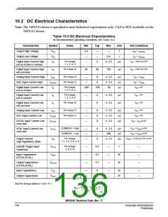
Output High Source Current
VOH = 2.4V (VOH min.)
Pin Groups 1, 2, 3
Pin Groups 5, 6, 7
Pin Groups 8
mA
I
—
—
—
—
—
—
-40
—
—
—
—
—
—
—
-4
-8
OH
-12
4
Output Low Sink Current
Pin Groups 1, 2, 3, 4
Pin Groups 5, 6, 7
Pin Group 8
mA
I
OL
VOL = 0.4V (VOL max)
8
12
125
Ambient Operating Temperature
(Automotive)
°C
T
A
Ambient Operating Temperature
(Industrial)
105
—
°C
T
-40
10,000
10,000
15
—
—
—
—
A
Flash Endurance (Automotive)
(Program Erase Cycles)
TA = -40°C to 125°C
TA = -40°C to 105°C
TJ <= 85°C avg
Cycles
Cycles
Years
N
F
Flash Endurance (Industrial)
(Program Erase Cycles)
N
—
F
Flash Data Retention (Automotive)
T
—
R
Note: Total chip source or sink current cannot exceed 200mA
See Pin Groups listed in Table 10-1
56F8345 Technical Data, Rev. 17
Freescale Semiconductor
Preliminary
135

 FREESCALE [ Freescale ]