DC Electrical Characteristics
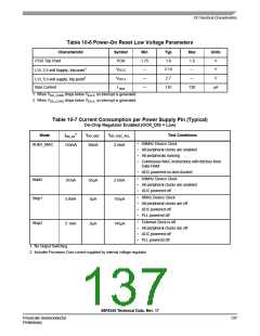
Table 10-6 Power-On Reset Low Voltage Parameters
Characteristic
POR Trip Point
Symbol
Min
Typ
Max
Units
POR
1.75
—
1.8
1.9
—
V
V
LVI, 2.5 volt Supply, trip point1
VEI2.5
2.14
LVI, 3.3 volt supply, trip point2
Bias Current
VEI3.3
I bias
—
—
2.7
—
V
110
130
μA
1. When V
2. When V
drops below V
drops below V
, an interrupt is generated.
, an interrupt is generated.
DD_CORE
DD_CORE
EI2.5
EI3.3
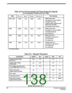
Table 10-7 Current Consumption per Power Supply Pin (Typical)
On-Chip Regulator Enabled (OCR_DIS = Low)
1
IDD_ADC
IDD_OSC_PLL
Mode
Test Conditions
• 60MHz Device Clock
IDD_IO
RUN1_MAC
155mA
50mA
2.5mA
• All peripheral clocks are enabled
• All peripherals running
• Continuous MAC instructions with fetches from
Data RAM
• ADC powered on and clocked
• 60MHz Device Clock
Wait3
Stop1
91mA
65μA
0μA
2.5mA
• All peripheral clocks are enabled
• ADC powered off
• 8MHz Device Clock
• All peripheral clocks are off
• ADC powered off
5.8mA
155μA
• PLL powered off
• External Clock is off
• All peripheral clocks are off
• ADC powered off
Stop2
5.1mA
0μA
145μA
• PLL powered off
1. No Output Switching
2. Includes Processor Core current supplied by internal voltage regulator
56F8345 Technical Data, Rev. 17
Freescale Semiconductor
Preliminary
137

 FREESCALE [ Freescale ]