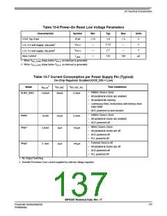
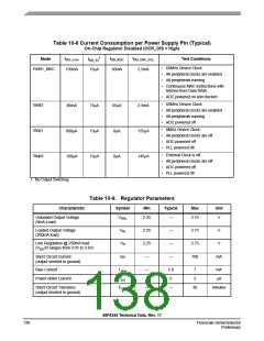
Table 10-8 Current Consumption per Power Supply Pin (Typical)
On-Chip Regulator Disabled (OCR_DIS = High)
1
IDD_Core
IDD_ADC
IDD_OSC_PLL
Mode
Test Conditions
• 60MHz Device Clock
IDD_IO
RUN1_MAC
150mA
13μA
50mA
2.5mA
• All peripheral clocks are enabled
• All peripherals running
• Continuous MAC instructions with
fetches from Data RAM
• ADC powered on and clocked
• 60MHz Device Clock
• All peripheral clocks are enabled
• All peripherals running
• ADC powered off
Wait3
Stop1
Stop2
86mA
800μA
100μA
13μA
13μA
13μA
65μA
0μA
2.5mA
155μA
145μA
• 8MHz Device Clock
• All peripheral clocks are off
• ADC powered off
• PLL powered off
• External Clock is off
• All peripheral clocks are off
• ADC powered off
0μA
• PLL powered off
1. No Output Switching
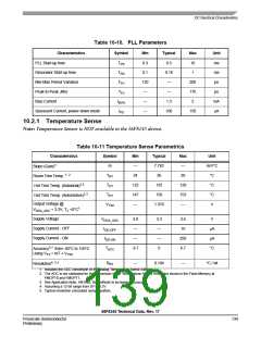
Table 10-9. Regulator Parameters
Characteristic
Symbol
Min
Typical
Max
Unit
Unloaded Output Voltage
(0mA Load)
VRNL
2.25
—
2.75
V
Loaded Output Voltage
(200mA load)
VRL
2.25
2.25
—
—
2.75
2.75
V
V
Line Regulation @ 250mA load
(VDD33 ranges from 3.0V to 3.6V)
VR
Short Circuit Current
Iss
—
—
700
mA
(output shorted to ground)
Bias Current
I bias
Ipd
—
—
—
5.8
0
7
2
mA
μA
Power-down Current
Short-Circuit Tolerance
TRSC
—
30
minutes
(output shorted to ground)
56F8345 Technical Data, Rev. 17
138
Freescale Semiconductor
Preliminary

 FREESCALE [ Freescale ]