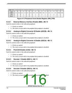
Base + $C
Read
15
14
13
12
11
10
9
8
7
6
5
4
3
2
1
0
EMI ADCB ADCA CAN DEC1 DEC0 TMRD TMRC TMRB TMRA SCI1 SCI0 SPI1
SPI0 PWMB PWMA
Write
1
1
1
1
1
1
1
1
1
1
1
1
1
1
1
1
RESET
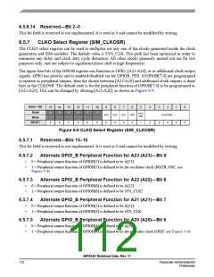
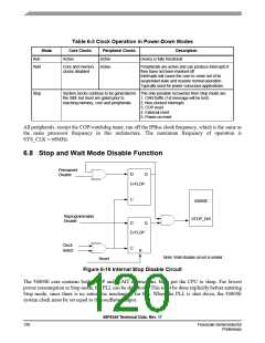
Figure 6-12 Peripheral Clock Enable Register (SIM_PCE)
6.5.9.1
External Memory Interface Enable (EMI)—Bit 15
Each bit controls clocks to the indicated peripheral.
•
•
1 = Clocks are enabled
0 = The clock is not provided to the peripheral (the peripheral is disabled)
6.5.9.2
Analog-to-Digital Converter B Enable (ADCB)—Bit 14
Each bit controls clocks to the indicated peripheral.
•
•
1 = Clocks are enabled
0 = The clock is not provided to the peripheral (the peripheral is disabled)
6.5.9.3
Analog-to-Digital Converter A Enable (ADCA)—Bit 13
Each bit controls clocks to the indicated peripheral.
•
•
1 = Clocks are enabled
0 = The clock is not provided to the peripheral (the peripheral is disabled)
6.5.9.4
FlexCAN Enable (CAN)—Bit 12
Each bit controls clocks to the indicated peripheral.
•
•
1 = Clocks are enabled
0 = The clock is not provided to the peripheral (the peripheral is disabled)
6.5.9.5
Decoder 1 Enable (DEC1)—Bit 11
Each bit controls clocks to the indicated peripheral.
•
•
1 = Clocks are enabled
0 = The clock is not provided to the peripheral (the peripheral is disabled)
6.5.9.6
Decoder 0 Enable (DEC0)—Bit 10
Each bit controls clocks to the indicated peripheral.
•
•
1 = Clocks are enabled
0 = The clock is not provided to the peripheral (the peripheral is disabled)
56F8345 Technical Data, Rev. 17
116
Freescale Semiconductor
Preliminary

 FREESCALE [ Freescale ]