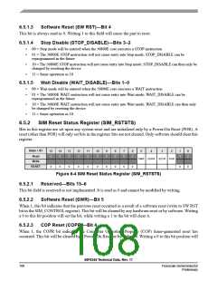
6.5.6.14 Reserved—Bit 2–0
This bit field is reserved or not implemented. It is read as 0 and cannot be modified by writing.
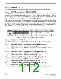
6.5.7
CLKO Select Register (SIM_CLKOSR)
The CLKO select register can be used to multiplex out any one of the clocks generated inside the clock
generation and SIM modules. The default value is SYS_CLK. This path has been optimized in order to
minimize any delay and clock duty cycle distortion. All other clocks primarily muxed out are for test
purposes only, and are subject to significant phase shift at high frequencies.
The upper four bits of the GPIOB register can function as GPIO, [A23:A20], or as additional clock output
signals. GPIO has priority and is enabled/disabled via the GPIOB_PER. If GPIOB[7:4] are programmed
to operate as peripheral outputs, then the choice between [A23:A20] and additional clock outputs is done
here in the CLKOSR. The default state is for the peripheral function of GPIOB[7:4] to be programmed as
[A23:A20]. This can be changed by altering [A23:A20], as shown in Figure 6-9.
Base + $A
15
0
14
0
13
0
12
0
11
0
10
0
9
A23
0
8
A22
0
7
A21
0
6
A20
0
5
4
0
3
0
2
CLKOSEL
0
1
0
0
0
Read
Write
CLK
DIS
0
0
0
0
0
0
1
RESET
Figure 6-9 CLKO Select Register (SIM_CLKOSR)
6.5.7.1
Reserved—Bits 15–10
This bit field is reserved or not implemented. It is read as 0 and cannot be modified by writing.
6.5.7.2
Alternate GPIO_B Peripheral Function for A23 (A23)—Bit 9
•
•
0 = Peripheral output function of GPIOB[7] is defined to be A[23]
1 = Peripheral output function of GPIOB[7] is defined to be the oscillator clock (MSTR_OSC, see
Figure 3-4)
6.5.7.3
Alternate GPIO_B Peripheral Function for A22 (A22)—Bit 8
•
•
0 = Peripheral output function of GPIOB[6] is defined to be A[22]
1 = Peripheral output function of GPIOB[6] is defined to be SYS_CLK2
6.5.7.4
Alternate GPIO_B Peripheral Function for A21 (A21)—Bit 7
•
•
0 = Peripheral output function of GPIOB[5] is defined to be A[21]
1 = Peripheral output function of GPIOB[5] is defined to be SYS_CLK
6.5.7.5
Alternate GPIO_B Peripheral Function for A20 (A20)—Bit 6
•
•
0 = Peripheral output function of GPIOB[4] is defined to be A[20]
1 = Peripheral output function of GPIOB[4] is defined to be the prescaler clock (FREF, see Figure 3-4)
56F8345 Technical Data, Rev. 17
112
Freescale Semiconductor
Preliminary

 FREESCALE [ Freescale ]