Register Descriptions
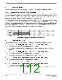
6.5.7.6
Clockout Disable (CLKDIS)—Bit 5
•
•
0 = CLKOUT output is enabled and will output the signal indicated by CLKOSEL
1 = CLKOUT is tri-stated
6.5.7.7
CLockout Select (CLKOSEL)—Bits 4–0
Selects clock to be muxed out on the CLKO pin.
•
•
•
•
•
•
•
•
•
00000 = SYS_CLK (from OCCS - DEFAULT)
00001 = Reserved for factory test—56800E clock
00010 = Reserved for factory test—XRAM clock
00011 = Reserved for factory test—PFLASH odd clock
00100 = Reserved for factory test—PFLASH even clock
00101 = Reserved for factory test—BFLASH clock
00110 = Reserved for factory test—DFLASH clock
00111 = Oscillator output
01000 = Fout (from OCCS)
•
•
•
•
•
•
•
•
•
01001 = Reserved for factory test—IPB clock
01010 = Reserved for factory test—Feedback (from OCCS, this is path to PLL)
01011 = Reserved for factory test—Prescaler clock (from OCCS)
01100 = Reserved for factory test—Postscaler clock (from OCCS)
01101 = Reserved for factory test—SYS_CLK2 (from OCCS)
01110 = Reserved for factory test—SYS_CLK_DIV2
01111 = Reserved for factory test—SYS_CLK_D
10000 = ADCA clock
10001 = ADCB clock
6.5.8
GPIO Peripheral Select Register (SIM_GPS)
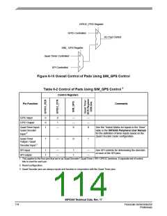
The GPIO Peripheral Select Register can be used to multiplex out any one of the three alternate peripherals
for GPIOC. The default peripheral is Quad Decoder 1 and Quad Timer B (NOT available in the 56F8145
device); these peripherals work together.
The four I/O pins associated with GPIOC can function as GPIO, Quad Decoder 1/Quad Timer B, or as
SPI 1 signals. GPIO is not the default and is enabled/disabled via the GPIOC_PER, as shown in
Figure 6-10 and Table 6-2. When GPIOC[3:0] are programmed to operate as peripheral I/O, then the
choice between decoder/timer and SPI inputs/outputs is made in the SIM_GPS and in conjunction with the
Quad Timer Status and Control Registers (SCR). The default state is for the peripheral function of
GPIOC[3:0] to be programmed as decoder functions. This can be changed by altering the appropriate
controls in the indicated registers.
56F8345 Technical Data, Rev. 17
Freescale Semiconductor
Preliminary
113

 FREESCALE [ Freescale ]