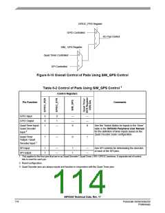
GPIOC_PER Register
GPIO Controlled
0
1
I/O Pad Control
SIM_ GPS Register
0
1
Quad Timer Controlled
SPI Controlled
Figure 6-10 Overall Control of Pads Using SIM_GPS Control
1
Table 6-2 Control of Pads Using SIM_GPS Control
Control Registers
Pin Function
Comments
GPIO Input
0
0
1
0
1
—
—
0
—
—
0
GPIO Output
Quad Timer Input /
Quad Decoder
—
See the “Switch Matrix for Inputs to the Timer”
table in the 56F8300 Peripheral User Manual
for the definition of timer inputs based on the
Quad Decoder mode configuration.
Input 2
Quad Timer
1
—
0
1
Output / Quad
Decoder Input 3
SPI input
1
1
—
—
1
1
—
—
See SPI controls for determining the direction
of each of the SPI pins.
SPI output
1. This applies to the four pins that serve as Quad Decoder / Quad Timer / SPI / GPIOC functions. A separate set of control
bits is used for each pin.
2. Reset configuration
3. Quad Decoder pins are always inputs and function in conjunction with the Quad Timer pins.
56F8345 Technical Data, Rev. 17
114
Freescale Semiconductor
Preliminary

 FREESCALE [ Freescale ]