Register Descriptions
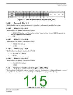
Base + $B
Read
15
0
14
0
13
0
12
0
11
0
10
0
9
0
8
0
7
0
6
0
5
0
4
0
3
C3
0
2
C2
0
1
C1
0
0
C0
0
Write
0
0
0
0
0
0
0
0
0
0
0
0
RESET
Figure 6-11 GPIO Peripheral Select Register (SIM_GPS)
6.5.8.1
Reserved—Bits 15–4
This bit field is reserved or not implemented. It is read as 0 and cannot be modified by writing.
6.5.8.2
GPIOC3 (C3)—Bit 3
This bit selects the alternate function for GPIOC3.
•
•
0 = HOME1/TB3 (default - see “Switch Matrix Mode” bits of the Quad Decoder DECCR register in the
56F8300 Peripheral User’s Manual)
1 = SS1
6.5.8.3
GPIOC2 (C2)—Bit 2
This bit selects the alternate function for GPIOC2.
•
•
0 = INDEX1/TB2 (default)
1 = MISO1
6.5.8.4
GPIOC1 (C1)—Bit 1
This bit selects the alternate function for GPIOC1.
•
•
0 = PHASEB1/TB1 (default)
1 = MOSI1
6.5.8.5
GPIOC0 (C0)—Bit 0
This bit selects the alternate function for GPIOC0.
•
•
0 = PHASEA1/TB0 (default)
1 = SCLK1
6.5.9
Peripheral Clock Enable Register (SIM_PCE)
The Peripheral Clock Enable register is used to enable or disable clocks to the peripherals as a power
savings feature. The clocks can be individually controlled for each peripheral on the chip.
56F8345 Technical Data, Rev. 17
Freescale Semiconductor
Preliminary
115

 FREESCALE [ Freescale ]