Clock Generation Overview
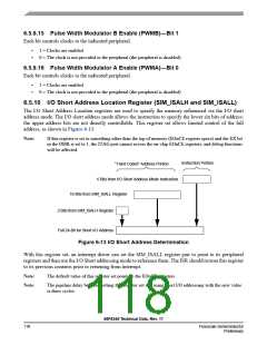
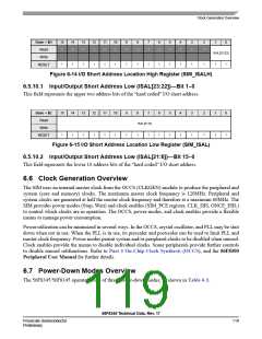
Base + $D
Read
15
1
14
1
13
1
12
1
11
1
10
1
9
1
8
1
7
1
6
1
5
1
4
1
3
1
2
1
1
0
ISAL[23:22]
Write
1
1
1
1
1
1
1
1
1
1
1
1
1
1
1
1
RESET
Figure 6-14 I/O Short Address Location High Register (SIM_ISALH)
6.5.10.1 Input/Output Short Address Low (ISAL[23:22])—Bit 1–0
This field represents the upper two address bits of the “hard coded” I/O short address.
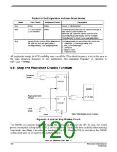
Base + $E
Read
15
1
14
1
13
1
12
1
11
1
10
1
9
1
8
7
6
1
5
1
4
1
3
1
2
1
1
1
0
1
ISAL[21:6]
Write
1
1
RESET
Figure 6-15 I/O Short Address Location Low Register (SIM_ISAL)
6.5.10.2 Input/Output Short Address Low (ISAL[21:6])—Bit 15–0
This field represents the lower 16 address bits of the “hard coded” I/O short address.
6.6 Clock Generation Overview
The SIM uses an internal master clock from the OCCS (CLKGEN) module to produce the peripheral and
system (core and memory) clocks. The maximum master clock frequency is 120MHz. Peripheral and
system clocks are generated at half the master clock frequency and therefore at a maximum 60MHz. The
SIM provides power modes (Stop, Wait) and clock enables (SIM_PCE register, CLK_DIS, ONCE_EBL)
to control which clocks are in operation. The OCCS, power modes, and clock enables provide a flexible
means to manage power consumption.
Power utilization can be minimized in several ways. In the OCCS, crystal oscillator, and PLL may be shut
down when not in use. When the PLL is in use, its prescaler and postscaler can be used to limit PLL and
master clock frequency. Power modes permit system and/or peripheral clocks to be disabled when unused.
Clock enables provide the means to disable individual clocks. Some peripherals provide further controls
to disable unused subfunctions. Refer to Part 3 On-Chip Clock Synthesis (OCCS), and the 56F8300
Peripheral User Manual for further details.
6.7 Power-Down Modes Overview
The 56F8345/56F8145 operate in one of three power-down modes, as shown in Table 6-3.
56F8345 Technical Data, Rev. 17
Freescale Semiconductor
Preliminary
119

 FREESCALE [ Freescale ]