Controller Area Network (CAN) Timing
.
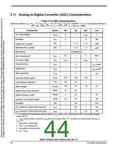
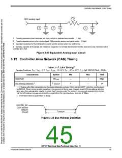
ADC analog input
3
1
2
4
1. Parasitic capacitance due to package, pin to pin, and pin to package base coupling. (1.8pf)
2. Parasitic capacitance due to the chip bond pad, ESD protection devices and signal routing. (2.04pf)
3. Equivalent resistance for the ESD isolation resistor and the channel select mux. (500 ohms)
4. Sampling capacitor at the sample and hold circuit. Capacitor 4 is normally disconnected from the input and is only connected to it at
sampling time. (1pf)
Figure 3-27 Equivalent Analog Input Circuit
3.12 Controller Area Network (CAN) Timing
2
Table 3-17 CAN Timing
DD
Operating Conditions: V = V
= 0 V, V = V
= 3.0–3.6 V, T = –40° to +85°C, C < 50pF, MSCAN Clock = 30MHz
SS
SSA
DDA A L
Characteristic
Symbol
Min
—
5
Max
Unit
Baud Rate
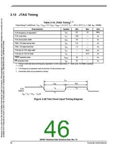
Bus Wakeup detection 1
BRCAN
1
Mbps
T WAKEUP
μs
—
1. If Wakeup glitch filter is enabled during the design initialization and also CAN is put into SLEEP mode then, any bus event
(on MSCAN_RX pin) whose duration is less than 5 microseconds is filtered away. However, a valid CAN bus wakeup detection
takes place for a wakeup pulse equal to or greater than 5 microseconds. The number 5 microseconds originates from the fact
that the CAN wakeup message consists of 5 dominant bits at the highest possible baud rate of 1Mbps.
2. Parameters listed are guaranteed by design
MSCAN_RX
CAN receive
data pin
T WAKEUP
(Input)
Figure 3-28 Bus Wakeup Detection
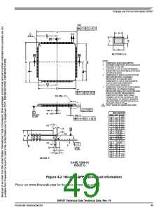
56F807 Technical Data Technical Data, Rev. 16
Freescale Semiconductor
45

 FREESCALE [ Freescale ]