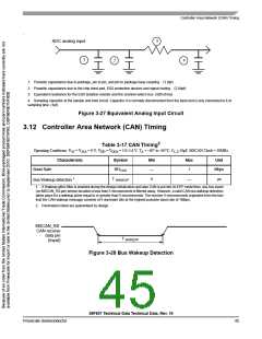
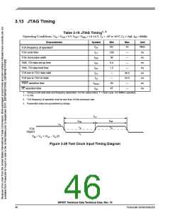
Serial Communication Interface (SCI) Timing
3.10 Serial Communication Interface (SCI) Timing
4
Table 3-15 SCI Timing
Operating Conditions: VSS = VSSA = 0 V, VDD = VDDA = 3.0–3.6 V, TA = –40° to +85°C, CL ≤ 50pF, fOP = 80MHz
Characteristic
Symbol
Min
—
Max
Unit
Baud Rate1
BR
(fMAX*2.5)/(80)
Mbps
RXD2 Pulse Width
TXD3 Pulse Width
RXDPW
TXDPW
0.965/BR
1.04/BR
1.04/BR
ns
ns
0.965/BR
1. fMAX is the frequency of operation of the system clock in MHz.
2. The RXD pin in SCI0 is named RXD0 and the RXD pin in SCI1 is named RXD1.
3. The TXD pin in SCI0 is named TXD0 and the TXD pin in SCI1 is named TXD1.
4. Parameters listed are guaranteed by design.
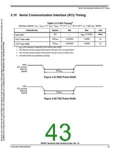
RXD
SCI receive
data pin
RXDPW
(Input)
Figure 3-25 RXD Pulse Width
TXD
SCI receive
data pin
TXDPW
(Input)
Figure 3-26 TXD Pulse Width
56F807 Technical Data Technical Data, Rev. 16
Freescale Semiconductor
43

 FREESCALE [ Freescale ]