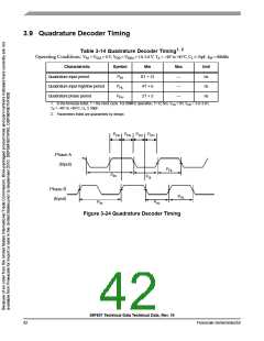
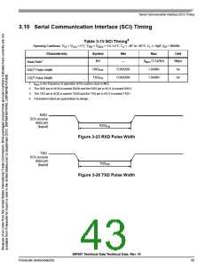
Quad Timer Timing
3.8 Quad Timer Timing
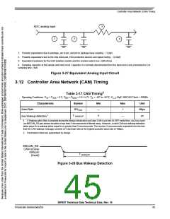
1, 2
Table 3-13 Timer Timing
Operating Conditions: VSS = VSSA = 0 V, VDD = VDDA = 3.0–3.6 V, TA = –40° to +85°C, CL ≤ 50pF, fOP = 80MHz
Characteristic
Timer input period
Symbol
PIN
Min
4T + 6
2T + 3
2T
Max
—
Unit
ns
Timer input high/low period
Timer output period
PINHL
POUT
—
ns
—
ns
Timer output high/low period
POUTHL
1T
—
ns
1. In the formulas listed, T = the clock cycle. For 80MHz operation, T = 12.5ns.
2. Parameters listed are guaranteed by design.
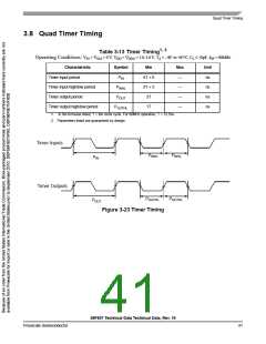
Timer Inputs
PINHL
PINHL
PIN
Timer Outputs
POUTHL
POUTHL
POUT
Figure 3-23 Timer Timing
56F807 Technical Data Technical Data, Rev. 16
Freescale Semiconductor
41

 FREESCALE [ Freescale ]